Balancing energy efficiency and ease-of-use in a world of high power demands
A universal solution for both high and low power applications
We are surrounded by electrically powered devices. The mobile phones in our pockets, the laptop computers we use on the job, the television in our living rooms, the servers powering the Internet, or even the EV car in our garage - all require electricity to operate and drive the demand for power supplies which are more efficient, smaller, and cheaper than before. This need for improved power density and highest efficiency at an affordable cost is pushing designers to find new and innovative solutions which are easy to implement in a broad range of low and high power applications while still meeting the rapidly increasing and very demanding design requirements.
One of the first places to work on resolving the challenges power systems designers face is efficiency. Higher efficiency means that less waste heat is generated which reduces cooling requirements and enables size reductions as well as energy cost savings.
The starting point for developing dense and efficient power systems is the selection of a suitable topology. The performance of the core power components in the topology typically is the key factor for the final performance. For a component maker this implies a focus on improving the key Figures of Merit (FoM) of the component and the efficiency gains that this provides. In addition other factors come into play which have significant impacts on size, density, and cost. Power switches in through-hole packages such as the popular TO-220 and TO-247 packages are still widely used. However, advances in semiconductor and packaging technology increasingly enable the use of surface mount devices (SMD) in ever expanding power classes. In particular the thermal management challenges historically blocking the use of SMD technology are becoming less and less critical with modern SMD components. This also helps to reduce space, production complexity, and cost. Finally, considering the ever increasing variety of power supply designs, one of the key features of a successful power switch for the broad market is its ease of design-in (ease-of-use). A component must work well in different application environments, showing good efficiency under various conditions, demanding little design effort to minimize unwanted effects such as voltage spikes or electromagnetic interference (EMI), and showing a solid robustness in abnormal conditions.
The SuperJunction concept
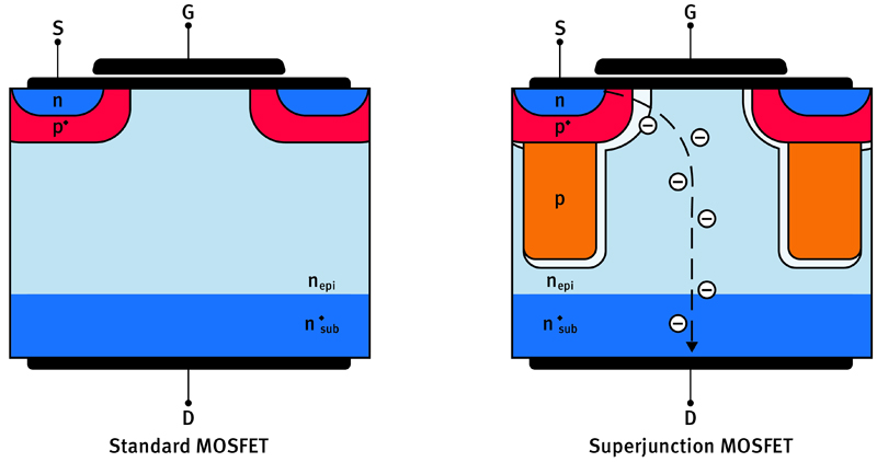
In 1999, Infineon introduced the CoolMOS™, a MOSFET drain structure design that beat the theoretical silicon limit line. This new SuperJunction (SJ) transistor design had two key features; the main current path (the n-region) was more heavily doped than in a traditional HV MOSFET, and the p-columns were precisely sized and doped to balance the n-region.
The heavily doped n-region lowers the on-state resistance, but has a side effect of a much lower blocking voltage capability. The p-columns compensate for this and balance out the current path, supporting a space charge region with zero net charge supporting high blocking voltage.

Click image to enlarge
Figure 1: Schematic drawing of conventional HV planar MOSFET and SJ MOSFET
This innovative construction of the SJ MOSFET allows a reduction in area specific resistance, and this in turn provides conduction loss benefits. The dramatic reduction in chip area for the first generation of CoolMOS™ technology lowered capacitance and dynamic losses as well.
The 600 V CoolMOS™ P7, efficiency in design
Since 1999, the CoolMOS™ technology has been refined over several generations cumulating in Infineon’s latest offering, the 600 V CoolMOS™ P7. This latest step in SuperJunction MOSFET improvement is based on the 600 V CoolMOS™ C7 platform and designed as the successor to the CoolMOS™ P6 Series. Targeting the highest efficiency/high performance segment the CoolMOS™ C7 was designed for ultimate switching performance without any compromise in order to enable highest efficiency in all target applications including PFC and HV DC-DC stages such as LLC . In contrast the 600V CoolMOS™ P7 balances the fast switching behavior with a strong focus on the ease-of-use (e.g. low ringing) requirements to enable a fast and easy design-in, even in plug and play situations. It provides an excellent combination of features that makes it a perfect fit for a wide range of applications from low power consumer devices and PC power supplies all the way up to high power applications such as data centers, telecom, and EV chargers.
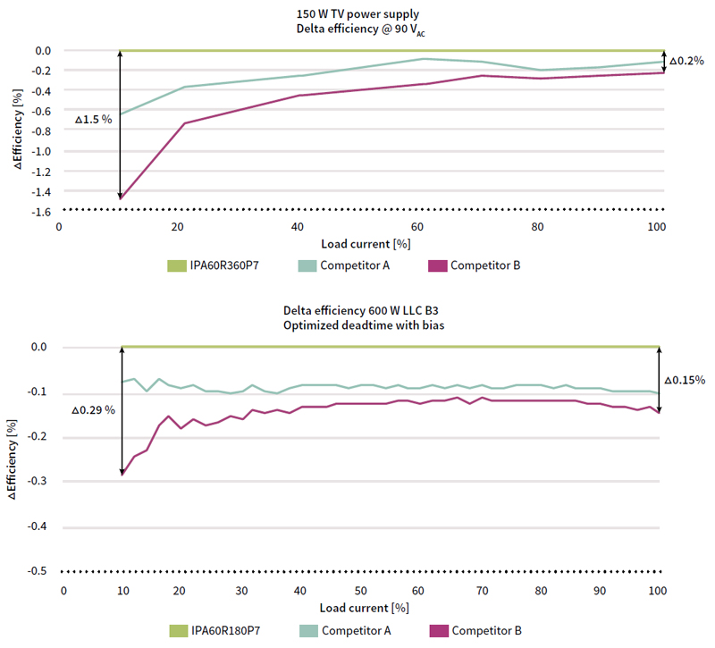
The 600V CoolMOS™ P7 provides an optimizedbalance between efficiency and ease-of-use at a competitive price. The gate charge Qg and Eoss are thirty to sixty percent lower compared to previous CoolMOS™ series minimizing driving and switching losses. These features combined with an optimized typical RDS(on) enable efficiency gains over the whole load range across the various power classes compared to the predecessor series.The 600V CoolMOS™ P7 shows up to 1.5 percent better efficiency and 4.2°C lower MOSFET temperature than comparable devices on the market.
Click image to enlarge
Figure 2: Efficiency of CoolMOS™ P7 versus competing devices
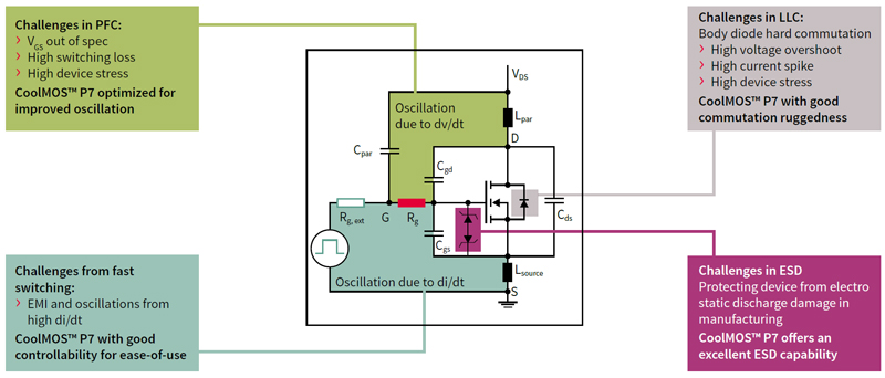
In LLC circuits the rugged body diode of the 600 V CoolMOS™ P7 protects the device during hard commutation events. The portfolio offers a very wide RDS(on) range from 37 mΩ to 600 mΩ and covers a variety of surface mount (SMD) and through hole packages. All parts come with an excellent ESD robustness of more than 2 kV (HBM) where for products with RDS(on) values higher than 100 mΩ the high ESD level is guaranteed by an integrated Zener diode.
Considering all these features enabling high efficiency and power density at minimum design effort and most competitive prices P7 is the perfect solution to the next generation of switched mode power supply designs for a broad range of application challenges.
Summary
The key features of the 600V CoolMOS™ P7 make it perfectly suited for a wide range of product designs ranging from low power SMPS right up to the highest power levels. The P7 provides ease-of-use and fast design-in supported by a low ringing tendency and can be used across PFC and PWM stages. Excellent efficiency FoMs, in particular the low switching and conduction losses (-50% Eoss, -30% Qg, -20% turn-off losses) guarantee highest efficiency and help to manage the thermal load of power supply solutions.
The unique ease-of-use properties of the 600 V CoolMOS™ P7 are the result of carefully selected and integrated gate resistors. In addition, 600V CoolMOS™ P7 has an outstanding body diode ruggedness which makes it the perfect fit not only for hard but also for soft switching applications (LLC). The excellent ESD robustness of greater than 2 kV (HBM) over the whole portfolio supports highest assembly yields.
Click image to enlarge
Figure 3: CoolMOS™ P7 meets most critical design challenges
The 600 V CoolMOS™ P7 is be available in nine different packages at an RDS(on) granularity from 37 mΩ to 600 mΩ. It is designed as a general purpose part addressing a broad range of applications with a single product family. The portfolio contains parts that are qualified to industrial grade as well as parts qualified to standard grade. This allows designers to choose the perfect device for the specific application requirements of a design and minimize the price tag. For high power density solutions 600 V CoolMOS™ P7 also offers best-in-class RDS(on) and package combinations. The 600 V CoolMOS™ P7 portfolio is completed by a 65mΩ device in ThinPAK 8x8 and a 60mΩ part in TO220(FP) making it a perfect choice for high power applications. For the low power arena, the 600 V CoolMOS™ P7 is offered in SOT223 which allows smaller application footprints and cost competitive solutions for the consumer market replacing actual DPAK solutions.
All together 600 V CoolMOS™ P7 combines eighteen years of super junction MOSFET innovation into Infineon‘s most rounded CoolMOS™ technology ever - giving the best balance between performance, ease of use and price to be found on the market today.