High power LEDs continue to proliferate in modern lighting systems, spanning automotive headlights, industrial/commercial signage, architectural lighting, and a variety of consumer electronics applications. The industry’s transition toward LED technology is driven by the distinct advantages that solid-state lighting offers over conventional light sources: the high efficiency conversion of electrical power to light output, as well as long operational life spans.
As LED lighting is incorporated into an expanding array of applications, the demand for higher LED currents for increased light output also grows. One of the biggest challenges for powering strings of high current LEDs is maintaining high efficiency in the power converter stage that is responsible for providing a well-regulated LED current. Inefficiency in the power converter presents itself in the form of unwanted heat, which originates from the switching elements of the current regulator circuitry.
The LT3762 is a synchronous boost LED controller designed to curtail the sources of efficiency loss common in high power step-up LED driver systems. This device’s synchronous operation minimizes the losses normally incurred from the forward voltage drop of a catch diode in an asynchronous dc-to-dc converter. This increased efficiency allows the LT3762 to deliver much higher output current than similar asynchronous step-up LED drivers, especially at low input voltages. In order to improve low input voltage operation, an on-board dc-to-dc regulator provides 7.5 V to the gate drive circuitry, even when the input drops below 7.5 V. The result of having a strong gate drive voltage source at low input voltages is that the MOSFETs generate less heat as the input voltage decreases, which extends the low end of the operational input range to 3 V.
This step-up LED controller can be configured to operate between 100 kHz and 1 MHz fixed switching frequency, with optional −30% × fSW spread spectrum frequency modulation to reduce switching-related EMI energy peaks. The LT3762 can be run in a step-up, step-down, or step-up/step-down topology for powering LEDs. A high-side PMOS disconnect switch facilitates PWM dimming and protects the device from potential damage when the LEDs are placed in an open-/short-circuit condition.
The LT3762 features an internal PWM generator, which uses a single capacitor and a dc voltage to set the frequency and pulse width for up to a 250:1 PWM dimming ratio, and can alternatively use an external PWM signal to achieve ratios as high as 3000:1.
Synchronous Switching
In asynchronous dc-to-dc converter topologies, Schottky catch diodes are used as passive switches to simplify the control scheme of the converter to pulse-width modulating a single MOSFET. While this does simplify things from a control perspective, it limits the amount of current that can be delivered to the output. Schottky diodes, like PN junction devices, experience a forward voltage drop before any current can pass through the device. As the power dissipated in the Schottky diode is the product of its forward voltage drop and current, conduction-related power dissipation can result in several watts of loss at excessive output current levels, resulting in the Schottky diode heating up, which causes inefficiencies in the converter.
The LT3762 synchronous switching converter does not encounter the same output current limitations that asynchronous converters do. This is because synchronous converters replace the Schottky diode with a second MOSFET. Unlike Schottky diodes, MOSFETs do not have a forward voltage drop. Instead, MOSFETs feature a small resistance that is formed from drain to source when the device is fully enhanced. The conduction losses incurred from a MOSFET are much lower than with Schottky diodes at high current, as the power lost is proportional to the product of the square of the current through the device and drain-source resistance.
Low Input Voltage Operation
Another challenging region for high power boost LED controllers occurs during low input voltage operation. The majority of boost dc-to-dc regulator ICs use an internal LDO voltage regulator powered from the input of the device to provide lower voltage power to the analog and digital control circuitry within the IC. Of the circuitry that draws power from the internal LDO regulator, the gate driver consumes the most power, and its performance is affected by fluctuations in the output of the LDO regulator. As the input voltage drops below the LDO output voltage, the LDO output begins to collapse, which limits the gate driver’s ability to properly enhance the MOSFETs. When MOSFETs are not fully enhanced, they operate in a higher resistance state, causing them to dissipate power in the form of heat as current is passed through the device.
Low input voltage operation in step-up converter topologies results in higher input current, which, when having to pass through a more resistive MOSFET device, exacerbates conduction losses. Depending on the gate drive voltage of the regulator IC, this can severely limit the low input voltage range that the device can successfully achieve without overheating.
The LT3762 features an integrated buck-boost dc-to-dc regulator, instead of an LDO regulator, which provides 7.5 V to power the internal circuitry even when the input voltage is low. This buck-boost regulator only consumes three pins of the LT3762 IC, and requires only two additional components. Compared to internal LDO controller devices, which have minimum input voltages of 4.5 V and 6 V, the LT3762 is able to extend its input operating range down to 3 V. The 7.5 V output of the buck-boost converter supplies power to the gate driver, and allows for 6 V/7 V gate drive MOSFETs to be used. Higher gate drive voltage MOSFETs tend to have lower drain-source resistances, and (barring switching losses) operate more efficiently than their lower gate drive voltage counterparts.
Flexible Topologies
Like most other boost LED drivers from ADI, the LT3762 can be reconfigured to power LEDs in a step-up configuration, and also as a step-down (buck mode), and step-up/step-down (buck-boost mode and boost-buck mode). Of these boost converter topology variants, the ADI-patented boost-buck mode configuration offers the ability to operate as a step-up/step-down converter with the added benefit of low EMI operation. This topology utilizes two inductors, one input facing and the other output facing, to aid in filtering noise generated by switching. These inductors help suppress EMI from coupling to the input supply and the other devices that may be connected, as well as the LED load.
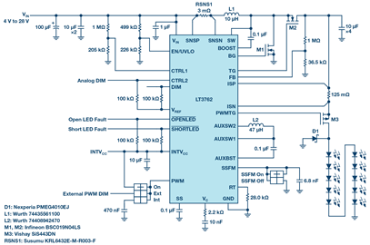
Additional circuitry can be added on to the boost-buck mode topology to offer short-circuit protection of the LED– node to GND. The schematic in Figure 5 shows the LT3762 in a boost-buck mode configuration with this protection circuitry added. In the event that LED– is shorted to GND, M4 is forced to turn off, blocking the conduction path to the input through the inductors and preventing excessive current draw. When M4 is forced to turn off, D3 pulls the EN/UVLO pin low to stop the converter from switching until the short circuit has been removed. The addition of this protective circuitry used in conjunction with the LT3762’s built-in open-/short-circuit detection results in a robust solution capable of surviving a variety of fault conditions in harsh environments.
Conclusion
Asynchronous boost converters often struggle to provide high output current without experiencing substantial power losses and heating of the catch diode under normal operation. In addition to loss generated by the Schottky diode, such converters struggle to maintain maximum power output capabilities as the input voltage decreases, which limits the power delivery across the input range. Asynchronous dc-to-dc converters are simply not suited for higher power levels, and a synchronous switching scheme must be implemented to meet application specifications. The LT3762 boost LED controller addresses the issues of delivering high output current with its synchronous switching, is capable of operating at much lower input voltages thanks to its onboard dc-to-dc converter, and has the flexibility to be used in a variety of circuit topologies.