Boosting Power Conversion in the Internet of Things
A highly integrated AC-DC buck converter with a universal input can boost the efficiency of devices during light load with low standby power mode across the IoT
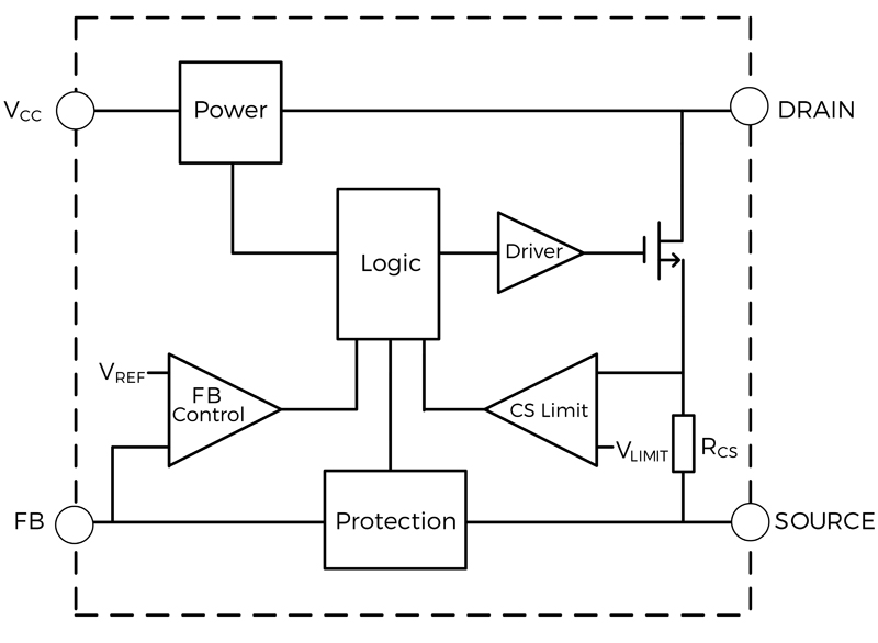
Figure 1: The functional block diagram of the AL17x50, integrating a MOSFET to reduce the BOM and improve the efficiency at low loads
The explosion in demand around the world for smart devices in the Internet of Things and the smart home means designers have to accommodate a wide range of power sources. These power sources have to cope with an even wider range of regulations.
At the same time, the end systems have to be as energy efficient as possible, putting even more strain on the design of the power system. This is not a simple challenge. The efficiency of a power converter varies significantly depending on the load. In the IoT and smart home, devices operate at light load for most of the time during standby mode and many converters are less efficient at these light load conditions. Similarly, converters that have to cope with a wide input voltage range from 90V to 264V and provide a highly stable output across a wide range of currents also tend to be less energy efficient.
Today’s IoT and connected lighting systems in the home need microcontrollers that run at low voltages and wireless links that need high currents quickly when transmitting. Wireless transceivers using the latest Bluetooth Low Energy (BLE), Zigbee and Wi-Fi protocols are often used to connect smart devices such as LED lighting to mobile phones or home hubs. These sit quiescent for most of the time but also need relatively high peak currents with stable regulated output voltage when transmitting or waking up from standby mode. This means there is a wide range of loading on the system.
All these factors present a major challenge for system designers. While integration in the power controller can provide the answer, it brings its own challenges.
Universal regulator
The AL17050 and AL17150 are universal AC high-voltage-input step-down regulators that integrate a MOSFET to deliver accurate constant voltage (CV) and dynamic performance without requiring an optocoupler over line and load regulation. Removing the optocoupler, along with a SOT-25 (AL17050) and SO7 (AL17150) package, means a significantly less complex design and smaller footprint. This works well for wireless nodes and LED lighting in smart home applications that need connectivity in a small space without excessive power consumption.
The regulator works with a single winding inductor so that fewer external components are needed. This reduces both the bill of materials (BOM) and the design footprint and also helps with the certification in a greater number of global markets as the range of protection capabilities meets all the different market requirements without adding extra cost to the design.
The on-resistance, RDS(on), of the internal MOSFET in the controller is 30Ω (AL17050 typical) and 10Ω (AL17150 typical) , which helps provide high-efficiency operation at light loads and improves the overall average efficiency, suitable for an application from 0.1W to 3W.
Click image to enlarge
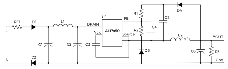
Figure 2: A typical application for the AL17x50 in a buck AC-DC power supply for smart home devices in the Internet of Things
Constant voltage
A key point is that the regulators provide a constant voltage (CV) output for the 3.3V/5V microcontrollers and wireless transceivers, ensuring that the end equipment is as reliable and energy-efficient as possible. The regulators can also supply other output voltage ratings, such as 15V, in IoT applications.
This is achieved by a control voltage that is provided by an internal high-voltage regulator. The chip starts up at 5.6V and the internal high-voltage regulator is turned off; when the voltage drops below 5.3V, the internal high-voltage regulator turns on again to charge an external capacitor. When the voltage drops below 3.4V, the IC stops and the internal high-voltage regulator charges the capacitor.
When the voltage of the regulator feedback pin is below the reference voltage (2.5V), the internal integrated MOSFET turns on. The peak current limit and the initial inductance current value together with the input voltage determine the on-time. When the current reaches peak current limit, the MOSFET turns off.
The output voltage can be controlled by sampling the voltage of the feedback pin, which is derived from the voltage of the sampling capacitor. In the off-stage of the MOSFET, when the inductor current drops below the output current, the sampling capacitor voltage begins to decrease. When the voltage of the feedback pin falls below the reference voltage (2.5V), a new switching cycle begins.
To maintain high efficiency under different load conditions, AL17050 and AL17150 adjust the switching frequency automatically.
As the load decreases, the switching frequency decreases and the MOSFET off-time increases, leading to the decrease of peak current. In no-load conditions, where a dummy load is retained, the frequency and the peak current are both minimized. This helps to reduce the power consumption under no-load conditions.
To improve load regulation and load-transient performance, the controller has an error amplifier (EA) compensation function. With an increasing load, the compensation value increases and the reference voltage of the internal feedback comparator is pulled down slightly. A faster change in the load will lead to a greater compensation step and then the output voltage will be regulated back to the desired voltage faster. This compensation will precisely maintain the output voltage.
Understanding the system performance helps optimize the design of the controller. For example, a narrow spike on the leading edge of the current waveform usually happens when the power MOSFET is turned on. A 350ns leading-edge blank is built into the controller to prevent the false-triggering caused by the turn-on spike. During this period, the current limit comparator is disabled and the gate driver cannot be switched off.
Protection
A wide range of protection features are essential for helping with certification in different global regulatory environments. In anticipation of these needs, the device has short-circuit protection (SCP), over-temperature protection (OTP), VCC under-voltage lock function (UVLO), over-load protection (OLP), and open-loop protection.
SCP enables the device to shut down when the peak current exceeds the threshold of 450mA, resuming operation when the fault is removed. As the load increases, the peak current and the switching frequency increase. When the peak current reaches the peak current limit value, the output voltage will decrease if the load continues to increase. When the feedback pin voltage drops below the OLP trigger threshold of 1.7V and this state is maintained for 170ms, the OLP occurs. Having this 170ms maintain time avoids triggering the OLP function when the power supply starts up or enters a load-transition phase, and therefore requires that the power supply starts up in less than 170ms.
Similarly, when the voltage on the feedback pin drops below 60mV, the device will stop working and begin a restart cycle. The open-loop detection is blanked for 64 switching cycles during the start-up stage.
The AL17050 and AL17150 integrate an internal thermal shutdown protection function. If the IC junction temperature rises above a typical value of +150°C, the thermal shutdown (TSD) protection is triggered and the internal MOSFET stops switching. To recover the switching of the internal MOSFET, the junction temperature has to fall by a hysteresis of +30°C below this value. During TSD protection, the main voltage drops to a restart value, typically 2.4V, and then the internal high-voltage regulator provides the main 3.3V/5V system voltage.
Conclusion
Higher integration delivers smaller, more efficient designs that can be used across many global applications and markets. This trend provides economies of scale and drives down costs, which is essential in high-volume smart home and IoT markets. A wide range of protection features allows designers to meet the regulatory requirements across those global markets, reducing development and test times.