Author:
By: Aleksey Pantsirev, Application Marketing Manager for Battery Chargers, Infineon Technologies
Date
10/18/2022
 PDF
PDF
Click image to enlarge
Figure 1. Infineon offering cover key components in chargers (colored in green)
Every day more and more of the devices and equipment used in our daily life are powered by batteries. For example, we can find electronic equipment with batteries around the house, such as cordless power tools, drones, and other domestic robots (e.g., robotic vacuum cleaners, lawnmowers, etc.). At the same time, due to rising fuel prices, government incentives, and rising awareness about air pollution, common modes of transportation such as bicycles, scooters, and mopeds have now also turned into electrical vehicles. All of these applications are swiftly changing the demands for battery charging equipment and infrastructure.
This article discusses how AC/DC battery charger reference designs up to 250 W can save design time and effort. Based on Infineon’s leading portfolio of high-voltage as well as low- and medium-voltage switches and power controllers, the ready-to-go reference designs can minimize design risks while meeting the requirements of advanced battery chargers.
What needs to be considered when designing an advanced battery charger
The essential operation of a battery charger is to convert the input AC voltage to an isolated DC voltage that restores the rechargeable battery’s capacity. Increasing power levels, higher safety requirements, and cost are major factors influencing today’s charger designs.
Some users can be more impatient, and thus fast charging has become a key point of differentiation. Chargers are expected to be able to charge advanced batteries in a reasonable time, which requires them to deliver high currents. At the same time, chargers play a vital role in the lifespan and reliability of the battery. When charging a battery at a high rate, it is critical to monitor its state of charge. Lithium-ion (Li-ion) batteries exhibit high-power density and low self-discharge, but they are much less tolerant to stress conditions than batteries based on other chemistries. Hence, battery chargers need to provide built-in protection features for over-charging, over-discharging, over-temperature, and excessive current events. Finally, as the charger is a relatively cost-sensitive application, the overall design cost needs to be justified to deliver winning products to market on time.
Battery charger design solutions for mobile appliances
Infineon’s offering for battery charging solutions is ranging from high-voltage CoolMOS™ superjunction MOSFETs, CoolGaN™ gate injection transistor (GIT) enhancement mode (e-mode) HEMTs to low- and medium-voltage (e.g., OptiMOS™ power MOSFETs) switches and dedicated controller ICs (Figure 1). The portfolio spans from ultra-high efficiency solutions to cost-performance oriented topologies. Based on an optimal selection of components and topologies, Infineon offers highly versatile reference designs for an accelerated time-to-market and reduced design risks. The reference designs come not only with schematics but also PCB data, Gerber files, and full characterization reports.
Flyback converter topology
The flyback converter is the most ubiquitous topology used in chargers. Its cost and simplicity make it a favorable solution over other topologies up to approximately 100 W. However, reliably controlling the flyback is not straightforward, and the controller IC needs to be fast and smart enough.
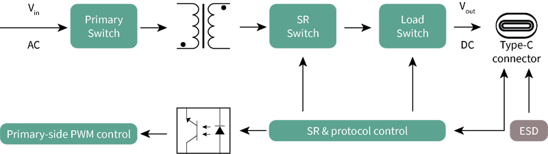
Infineon’s ICC80QSG flyback controller IC for battery charging was tailored for flyback topologies operating in quasi-resonant mode and valley switching discontinuous conduction mode (DCM) to achieve high power transfer efficiency across a wide operating range. Through advanced features like burst mode for very light loads, configurable hysteresis of brown-in and brown-out, as well as adjustable on-time mapping at valley changing position, the ICC80QSG controller significantly simplifies the implementation of safety features.
The 84 W AC-DC reference design for battery chargers (REF_ICC80QSG_84W1_BPA) (Figure 2) is an easy, robust, and cost-efficient design that combines the ICC80QSG controller with a single high-voltage 700 V CoolMOS™ P7 switch (IPN70R450P7S). The design achieves more than 90 percent efficiency at a full load condition and outputs DC voltage between 12 and 21 V. The board dissipates less than 200 mW no-load standby power and the CC output can be set from 0.4 to 4 A. Both semiconductor components are offered in small wave-solderable SMD packages. The solution fits common 12 V /18 V Li-ion battery packs used in power tools, e-bikes, and vacuum cleaners.
Click image to enlarge
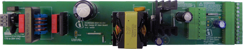
Figure 2: Top design image of the 84 W reference design
Another AC-DC topology that can be employed is hybrid flyback (HFB) which may also be referred to as asymmetrical resonant half-bridge. Hybrid flyback derives the principle of time-separated energy storage and transmission phase from the flyback topology while storing resonant energy for substantial energy transmission and zero voltage switching (ZVS) operation like LLC resonant converters. The main advantage of this topology is the extended energy storage approach which enables the usage of a smaller transformer at the same switching frequency compared to the standard and active clamp topologies. Zero voltage switching on the primary side and zero current switching (ZCS) on the secondary side are achieved by means of regulating both positive and negative magnetizing currents to increase efficiency.
The XDP™ XDPS2201 digital controller, designed specifically for this topology, enables (ultra) high-density charger designs and can work with either GaN HEMTs or silicon primary stage FETs. The XDP™ XDPS2201 hybrid flyback controller integrates a high voltage start-up cell and a high-side MOSFET gate driver leading to potential savings of up to 20 external components. The controller also offers a multi-mode operation across variable load- and line input conditions.
Infineon combined the XDP™ XDPS2201 controller with two 600 V CoolMOS™ P7 superjunction (SJ) MOSFETs (IPA60R280P7S) in a half-bridge configuration to design a 170 W high power density AC-DC design. The board shown in Figure 3 provides a wide output voltage range of 18 to 42 VDC and a charging current up to 4 A. The single-stage design demonstrates both high power density (16.5 W/in3) and high efficiency (94 percent). The board will be released at the end of 2022.
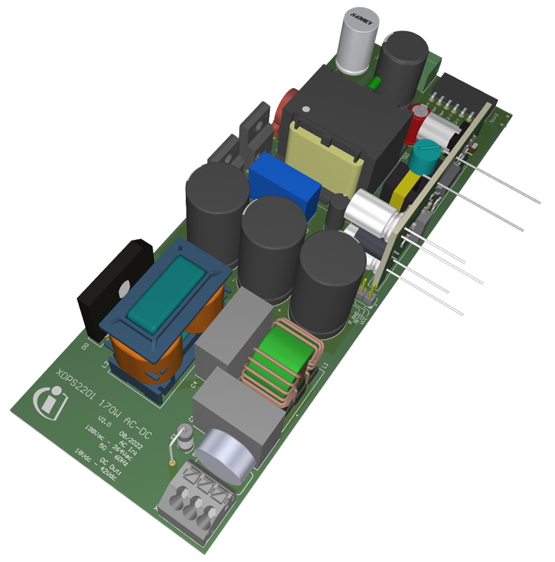
Click image to enlarge
Figure 3: Design image of the 170 W reference design with hybrid flyback topology
Hybrid flyback with GaN HEMTs
But the benefits of hybrid flyback (HFB) converter don’t stop there. If the silicon switches are replaced with GaN HEMTs, the amount of energy required to achieve zero-voltage switching is drastically reduced. Due to GaN’s fundamental advantages, such as outstanding specific dynamic on-state resistance and smaller switching losses, the switching frequency can be high, cutting the overall size of the charger.
Infineon will release a 140 W USB power delivery (PD) Type-C reference design that combines 600 V CoolGaN™ GIT HEMTs with the new XDP™ XDPS2221 HFB controller (coming soon) and the programmable EZ-PD™ CCG3PA USB-PD controller to achieve an industry-benchmark power density in this power range. The universal AC input (90 to 264 VAC) is converted into selectable 5 to 28 VDC by critical conduction mode PFC and hybrid flyback circuits. At just 110 mm x 38 mm x 23.5 mm, the reference design achieves not only an industry-benchmark power density of 23.35 W/in³ but also an outstanding peak efficiency of 95.1 percent (see Figure 4).
Click image to enlarge
Figure 4: 140 W ultra high-density USB-PD charger with 600 V CoolGaN™ HEMTs
LLC / LCC resonant converter
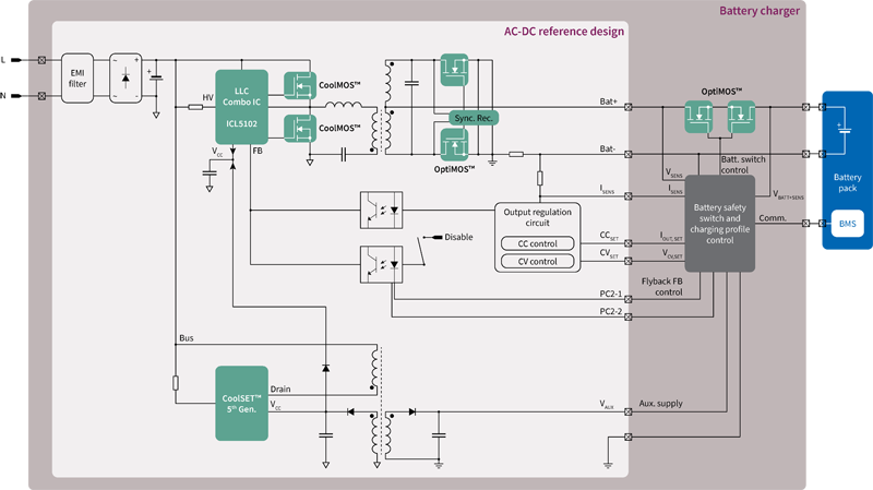
Battery chargers with a power range of a few hundred watts typically employ LLC or LCC resonant converter topology with a power factor correction (PFC) stage. Such designs can take advantage of the ICL5102 integrated PFC and resonant controller combo IC, designed to drive and control the boost PFC and resonant HB topology (LLC or LCC) together. By utilizing the coreless transformer technology, the IC can handle a high bus voltage of 650 V and supports a max operating frequency of 500 kHz, enabling a considerable size reduction of the transformer. The 600 V CoolMOS™ P7 superjunction MOSFET family is an ideal match for the combo controller.
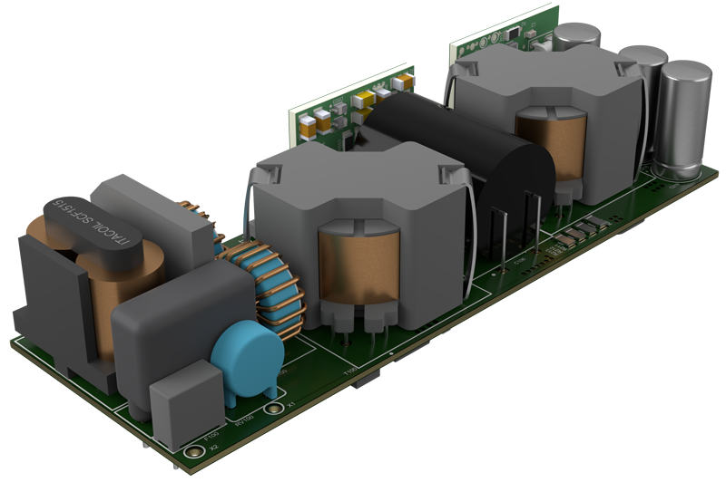
Another reference design that showcases the benefits of ICL5102 combo-controller IC and CoolMOS™ MOSFETs is coming in early 2023. As shown in Figure 5, the ICL5102 combo-controller is used to drive and control three power MOSFETs. With a total power output of 250 W, the design takes a universal AC input and converts it into 18 V to 42 VDC voltage with 93 percent efficiency at full load.
Click image to enlarge
Figure 5: 250 W reference design with LLC resonant topology
USB-PD bi-directional charging
USB PD revision 3.1 enables the delivery of up to 240 W, sufficient to charge numerous battery-powered applications within a reasonable time. The battery packs contain a USB-C connector which allows charging the battery pack with a USB-C charger (sink mode, the battery “sinks” power), or alternatively, the battery can charge a mobile phone (source mode, the battery “sources” power).
The EZ-PD™ PMG1 (Power Delivery Microcontroller Gen 1) portfolio of high-voltage MCUs is a prime choice for high-voltage USB PD sink or bi-directional sink/source solutions. In addition to the Arm® Cortex® core and USB PD stack, the PMG1-B1 controller features an integrated buck-boost controller rendering it suitable for bi-directional USB-PD charging.
Conclusion
The electronics industry’s expansion is catalyzing the demand for battery chargers. The chargers need to be fast and safe while remaining cost-competitive. Infineon offers solutions to fit a large variety of charger topologies at a competitive price point. Infineon’s reference designs are based on an optimal selection of components and topology and offer highly versatile reference designs for a fast time-to-market and reduced design risks.
For more information, please browse our dedicated online contents. Click here.