Bringing WBG technology to the next level: Part 1 of 4 Editorial Series sponsored by Infineon: Wide bandgap reliability is all about understanding how and why failures happen
Testing and qualification processes that ensure reliability throughout a complete product lifecycle
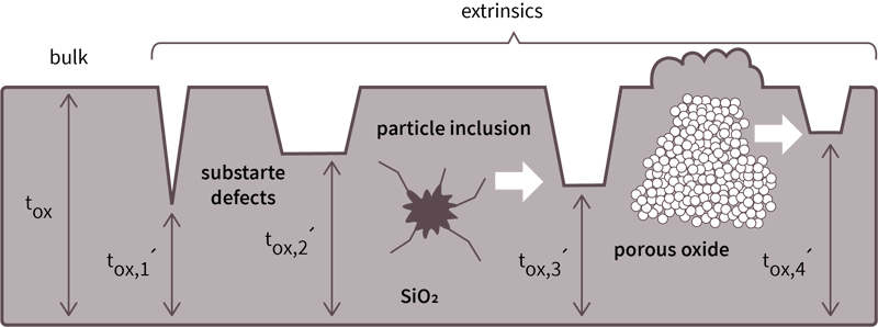
Figure 1. Examples for extrinsic defects in an amorphous layer, mathematically modeled via a local thinning effect in the gate-oxide of SiC devices
Introduction
The unique properties of Gallium Nitride (GaN) and Silicon Carbide (SiC) devices make them increasingly popular alternatives for silicon in power electronics applications. The appeal of SiC devices lies in their ability to offer unipolar device concepts with low switching losses at high voltages, while GaN devices can switch at much higher frequencies. Although these properties enable smaller and more power-efficient designs, mass production of these technologies has only recently become possible, which means little is known about their long-term performance in the field. While lifecycle modeling for silicon devices is well developed and can therefore be used as an accurate predictor of reliability, the different physical structure of wide bandgap devices means that a new approach to device lifecycle modeling is required.
In this article, we investigate the characteristics and behaviors of SiC and GaN devices that can impact their reliability. We also show the processes and testing procedures that Infineon has developed to help them predict the long-term behavior of their wide bandgap devices to ensure reliability in the field over the course of a full product lifecycle.
Understanding SiC device characteristics and failure mechanisms
Gate Oxide
SiC MOSFETs have a much higher extrinsic defect density, making them up to four times more likely to fail than silicon devices if no additional measures are applied. Extrinsic defects in the gate oxide can be modeled via a localized thinning effect which, for a given gate bias voltage, leads to a higher electric field that can cause the oxide to break down more quickly (Figure 1).
Infineon has developed innovative screening techniques, which are now used during testing to identify and remove potentially weak SiC devices. All parts are subjected to a stress pulse pattern designed to cause those with critical extrinsic defects to fail while allowing non-defective devices to continue functioning normally.
Bias temperature instabilities also impact reliability because high electric fields across the gate oxide cause device threshold voltage and, consequently, on-resistance to drift, leading to the potential for a thermal runaway to occur. While temperature instabilities caused by static voltages are well understood, transient device switching also contributes to drift in SiC device threshold voltage. The amount of drift depends on the turn-on bias voltage and the switching frequency. Still, these can be mitigated by ensuring that a device always remains within its safe operating area (SOA). Infineon recently introduced a technologically refined gate oxide formation process that largely eliminates dynamic drift’s impact on the threshold voltage instability.
Body diode
The body diode of a SiC MOSFET may experience bipolar degradation due to defects that originate mainly from the substrate material and penetrate the active layer (epi layer, drift zone). This can lead to the growth of stacking faults in the drift zone, which reduce the effective device area. These cause RDS(ON) to drift over time and the VSD of the body diode to increase. Stacking faults stop growing (saturate) once they reach the surface of the wafer, with the time taken for this to occur being dependent on the current through the PN junction and the junction temperature. Essential parameters like breakdown voltage, leakage currents, and switching behavior remain unaffected. Infineon has optimized its production process to suppress stacking fault formation. Devices that develop stacking faults can be detected and eliminated using additional screening tests applied to a finished device complementing the technological measures mentioned above. Those measures enable the long-term operation of SiC devices without violating the datasheet limits.
Cosmic Rays
Power devices in blocking mode work under high internal electric fields. In the case of SiC, those are about 10 times higher than in silicon. Particles originating from cosmic sources, which are present permanently in our atmosphere, can penetrate the active region of power devices and might result in a local carrier multiplication event that leads to the eventual destruction of the device – a Single Event Burnout (SEB). Robustness against SEB under a given applied reverse bias is improved by increasing the thickness and lowering the doping of the base layer. While this ensures a higher avalanche breakdown voltage, it comes with the caveat of higher on-state losses. Failure rates due to cosmic radiation increase exponentially with altitude, so it is important that calculations are performed specific to the device application, including applied voltage, altitude, and the required lifetime of the application. Infineon’s team of experienced application engineers can assist in the calculation of overall failure rates based on test data, application details, and the mission profile. In addition, the devices are designed to fulfill demanding failure rate requirements based on worst-case mission profiles for the major target applications.
Validating robustness
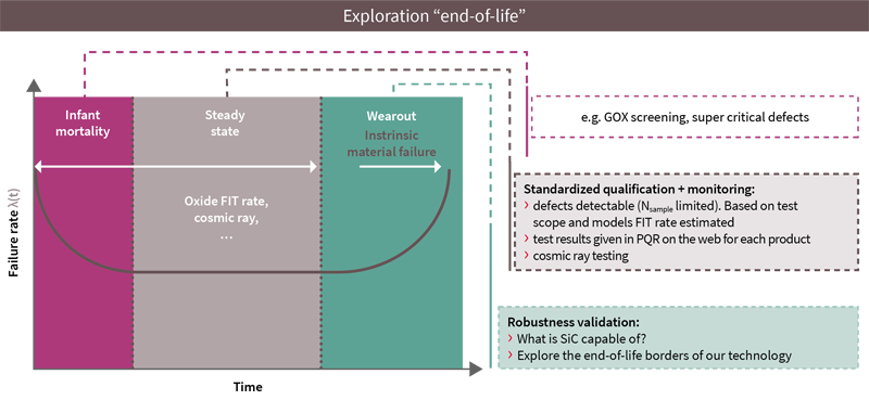
Infineon has developed a quality assurance program based on 25 years-experience in SiC-based power devices and shapes by its participation in several standards-development bodies, such as JEDEC international guidelines. This approach is designed to emulate the “bathtub” curve that describes the whole product lifecycle (Figure 2). Initial intensive screening attempts to eliminate devices with high defect levels, with all devices being regularly tested. All standardized tests are performed once for a minimum of 1,000 hours and were later extended up to 5,000 hours, well beyond the duration required for the relevant standards, allowing potential end-of-life behaviors to be captured. This comprehensive approach to validating device robustness has not identified any systematic end-of-life mechanisms, thereby ensuring that all CoolSiC™ MOSFETs exhibit exceptional levels of reliability.
Click image to enlarge
Figure 2. Emulating the “bathtub” curve, which represents the whole product lifecycle
Understanding GaN device behavior and failure mechanisms
Based on a high electron mobility transistor (HEMT) device structure, GaN devices behave very differently from their silicon-based counterparts. These differences can make GaN HEMT devices more sensitive than silicon when subjected to various stresses in power conversion applications.
Application testing profile
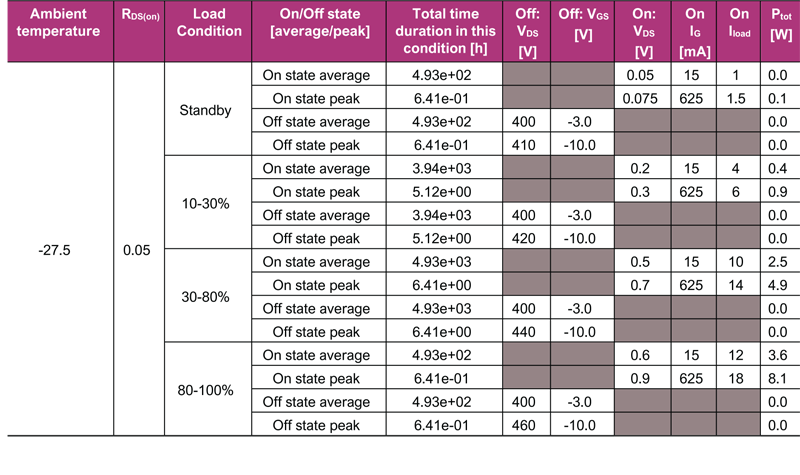
In qualifying these devices, Infineon uses an application-specific method to identify potential failure modes. For example, telecom rectifier (AC-DC) sockets endure stressful operating conditions in which they are required to operate for long durations at widely varying ambient temperatures that can reach high levels. Since this application represents a typical use case for GaN devices, Infineon chose to use it to qualify their GaN devices. Table 1 provides a high-level summary for device switching operation of power transistors in the power factor correction (PFC) section of a 2.5 kW telecom rectifier system.
Click image to enlarge
Table 1. Device switching operation (voltage and current data shown for one temperature) for telecom rectifier application
Drain-to-source bias voltage sensitivity
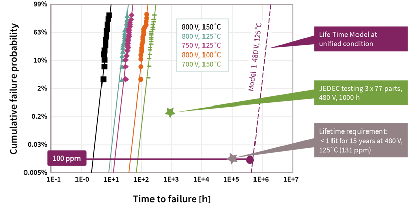
GaN HEMT devices, when tested under accelerated (beyond nominal rated values) voltage and temperature conditions, exhibit a failure rate that strongly correlates with drain-to-source bias voltage – the higher the drain-to-source bias voltage, the more quickly failure begins to occur. For example, in a sample of devices tested at 800 V and 125°C, all failed in just over 30 hours. For lower bias and temperature, longer duration before failure occurs. The tested values are used to project failure at use conditions: at 480 V and 125°C, failure is not projected to occur before approximately 2 million hours (Figure 3).
Even though GaN devices can withstand voltage stress much higher than their silicon counterparts, their lifetime at higher voltages is reduced. The model shows a lifetime greater than three times the target. The green star on the graph indicates the typical qualification time and failure fraction that can be detected using qualification methods currently used for silicon (but which are insufficient to predict the useful life of GaN devices). The grey star represents a target lifetime of 15 years at 100 failing parts per million (ppm).
Click image to enlarge
Figure 3. Cumulative fraction of sample failure vs. failure time for DC Bias (5 series on the left) and model for devices operating at 480 V, 125°C (dashed line)
Hard switching
SOA switching, also known as dynamic high temperature operating life (DHTOL), is another important mechanism that degrades the performance of GaN devices. Many GaN device manufacturers have published long-term application switching data, showing stable device operation (measured as steady case temperature) in hard switching applications over time durations ranging from 1,000 to 3,000 hours (18-60 weeks). However, this amount of time is insufficient to make conclusions about the performance of devices whose lifetime is intended to be in the order of many years.
To address this shortcoming, Infineon developed a test platform in which devices are operated at higher voltages and current than they were originally designed for to investigate if the reliability of devices in long-term hard switching operation could be predicted. This accelerated stress test circuit operates devices in a hard-switching boost configuration, like that used in PFC or other application circuits. The damage caused to devices under test conditions was controlled so that subsequent failure analysis could still be performed. The test platform uses a bus voltage up to 700 V (versus the typical use condition of 420 V) and higher than rated device currents. Beyond a certain threshold of peak voltages and currents, devices failures began to occur.
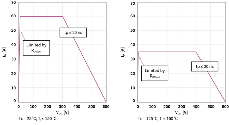
From this information, a model was extracted that allows failure rate as a function of current, voltage, and frequency to be predicted. The results of this model are shown in a repetitive switching SOA curve (Figure 4) that enables circuit designers to avoid operating devices with current and voltage combinations that threaten premature failure.
Click image to enlarge
Figure 4. Repetitive hard switching SOA curves identify the regions of operation to avoid premature failure
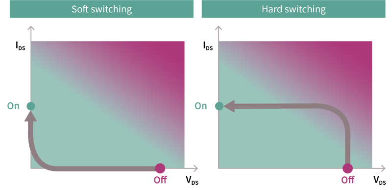
Accelerated testing was also performed on CoolGaN™ HEMTs operating in a soft-switching configuration like those used in DC-DC converters with an LLC architecture and other common topologies. No failures were observed at (or above) those operating conditions at which failures had previously occurred during accelerated hard switching. This illustrates that the switching locus plays a vital role in device failure (Figure 5).
Click image to enlarge
Figure 5. Soft switching prevents SOA failure, but caution must be taken with hard switching
Conclusion
The mass application of wide bandgap devices (SiC and GaN) has only relatively recently become possible, so there is little information about their reliability throughout a complete product lifecycle. Infineon’s deep understanding of the characteristics and behaviors of their CoolSiC™ and CoolGaN™ devices has allowed us to develop testing and qualification processes that are designed to prevent devices that could present a reliability concern from ever reaching the field.
To learn more about our innovative and broad product and technology portfolio of silicon-carbide- and gallium-nitride-based devices for applications with strong system performance demands, please visit our Wide-Bandgap Technology website.
References
[1] Infineon Technologies, “How Infineon controls and assures the reliability of SiC based power semiconductors”, Whitepaper, August 2020.
[2] Infineon Technologies, “Reliability and qualification of CoolGaN™, Technology and devices”, Whitepaper, October 2018.