Bringing WBG technology to the next level: Part 2 of 4 Editorial Series sponsored by infineon: Revolutionizing the next-gen power conversion applications
Superior efficiency and power density, combined with unmatched quality and supply stability
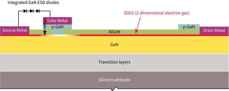
Figure 1. Cross-section view of Infineon’s CoolGaN™ GIT device structure
Introduction
Gallium Nitride (GaN) technology plays a major part in the wide bandgap revolution currently sweeping the semiconductor industry and manufacturers are racing to enter this burgeoning market. While the top-level advantages of using GaN devices in power electronics applications are clear (including higher switching frequencies, better performance at high temperatures, and lower power losses), the more subtle but nonetheless important differences between various GaN product offerings from different manufacturers are less so.
This article examines the many technological and logistical advantages of choosing Infineon’s CoolGaN™ GIT devices over similar devices available from other manufacturers.
Rugged and reliable gate structure
Figure 1 illustrates a cross-section of a CoolGaN™ gate injection transistor (GIT) HEMT device by Infineon. The diodes shown on the gate structure use a combination of titanium gate metal and p-GaN to form an ohmic contact to a GaN diode between the gate and source. This diode has a forward voltage of approximately 3.5 V. In addition, three serially connected GaN protection diodes are monolithically integrated into the GaN transistor to protect the gate from electrostatic discharge (ESD). These ESD diodes are designed to perform a clamping function if the gate-source voltage (VGS) exceeds -10 V in the reverse direction. The use of integrated diodes in both the forward and reverse direction means CoolGaN™ GIT devices are effectively self-clamping, making them extremely rugged and immune to damage from overvoltage spikes.
Superior RDS(on) and operating current
Figure 1 also shows the p-GaN “hybrid drain” structure adjacent to the drain metal in CoolGaN™ GIT devices. This structure effectively releases the trapped charge and helps mitigate the dynamic variation in RDS(on), which is an undesirable effect found in many GaN transistor designs from other manufacturers. Another technical advantage of a CoolGaN™ GIT device is its higher saturation current capability, especially at the maximum operating temperature (150°C).
Figure 2 compares the performance of a 70 mΩ-rated CoolGaN™ GIT HEMT 600 V and an alternative 650 V, 50 mΩ typical-rated device manufactured by a competitor. Even when driven to the maximum recommended gate voltage of 6 V, the alternative GaN is only rated for a maximum current of 25 A. By contrast, the CoolGaN™ device is rated for a 35 A maximum drain current and has lower RDS(on) over the entire current range. This peak current handling capability is critical because many applications require the device to withstand transient high-current conditions (startup, line-cycle dropout, lightning-strike transient, etc.).

Click image to enlarge
Figure 2. Infineon CoolGaN™ GIT device performance vs. competitor devices
This combination of a rugged gate structure and higher peak current handling capability contribute to making Infineon’s CoolGaN™ the most rugged and dependable GaN power transistor currently available.
System-level solution
Apart from GaN-on-silicon, Infineon is also developing silicon and silicon carbide (SiC) MOSFET devices. This broad-based approach to semiconductor device production demonstrates Infineon’s deep understanding of how to achieve the best performance from each technology in relevant applications.
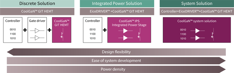
CoolGaN™ family features enhancement mode (normally-OFF) GIT HEMT devices as discrete and integrated power stage (IPS), which deliver efficiency improvements in typical power conversion applications. The operational benefits of these devices are derived from their ability to switch at remarkably high frequencies. However, these benefits can be hampered by the effects of parasitic impedance from the conventional package leads. To avoid this, Infineon leverages SMD (surface mount device) technology instead of through-hole packaging for its CoolGaN™ GIT devices, ensuring that the switching speed benefits can be fully realized. For more about packages with benefits for WBG semiconductors – click here.
Infineon’s series of CoolGaN™ GIT devices is additionally supported by a range of EiceDRIVER™ gate driver ICs, including isolated and non-isolated single- and dual-channel devices. The EiceDRIVER™ 1EDi and 2EDi families provide isolation between input and output channels enabling faster switching and more accurate timing.
Click image to enlarge
Figure 3. From flexible discrete to application-specific IPS system solutions
Device quality and reliability
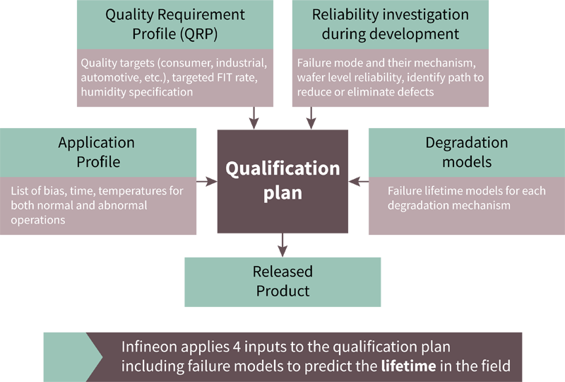
Infineon applies rigorous qualification and reliability test procedures to its CoolGaN™ GIT devices that are above and beyond standard JEDEC qualification to assure reliable operation in the field. Since mass production of GaN devices is a relatively recent phenomenon, it is important to develop an industry-standard methodology for device qualification. This will ensure a uniform approach to quality assurance so that customers do not need to investigate the procedures applied by individual manufacturers. To this end, Infineon has initiated and contributed to establishing a GaN-focused subcommittee (JC-70.1) within JEDEC to develop qualification guidelines and standards for GaN power devices.
Click image to enlarge
Figure 4.Infineon’s comprehensive four-part qualification plan for its CoolGaN™ GIT devices
Supply chain security
The demand for wide bandgap power semiconductors has increased considerably in recent years resulting in their supply constraints. Customers are now seeking additional reassurance on the delivery of high-quality and reliable devices on a regular basis, without supply chain interruptions, even as market demands continue to grow. As one of the world’s largest suppliers of power semiconductors, Infineon has a significant production capacity and a powerful market reputation for providing outstanding supply security. With in-house GaN epitaxy, the ability to perform frontend and backend processing, packaging, and testing, Infineon exerts full control over the supply chain for GaN devices – an approach that brought huge success for its silicon products.
Infineon continues to grow production capacity and recently opened a substantial 300 mm silicon fabrication facility in Villach, Austria. Once silicon production has been transferred to this new factory, existing 150- and 200-mm wafer production lines will then be rededicated to the production of GaN devices. Together with Infineon’s proven allocation management processes, this expanded capacity provides the flexibility and resources required for ultra-efficient processing and delivery of customer orders. In addition, further expansion of frontend capacity in Kulim, Malaysia, is already planned, creating room for the further significant growth of GaN epitaxial capacity. Recently Infineon decided to invest more than €2 billion to build a third production module at this site, aiming to add significant manufacturing capacities in the field of wide bandgap (SiC and GaN) semiconductors.
To prevent supply chain interruptions, Infineon implements a comprehensive business continuity management framework that encompasses all relevant business processes. Dedicated risk assessments are performed at each step of the value chain to ensure that potential risks are identified early and acted upon in a timely manner. After evaluation and categorization according to their level of impact and probability of occurrence, appropriate mitigation measures are applied. This framework also extends to suppliers who are evaluated according to their ability to meet Infineon’s exacting requirements. This ensures that the resources, tools, and support are available to ensure supply chain continuity in case of unforeseen events, including pandemics, geological and/or socio-political events, and raw material shortages.
Customer support
Infineon provides extensive technical support to its sales channels but also to customers via its self-service design support platform. During new product development, engineers develop appropriate and accurate technical documentation to explain device operation and features. These include product data sheets and a range of application notes which provide additional details about how to use new devices and benchmark their performance versus previous generation Infineon devices and competitor products. Infineon commonly provides application boards - available via its website (try the online Board Finder) and distribution partners - which enable customers to evaluate device performance.
In addition, a product registration environment (via myInfineon) is offered where customers can get full access to schematics, layout, bill of materials, and firmware for these application boards. Infineon also has dedicated, experienced, and trained teams of field application engineers (FAE) located in multiple regions and countries. This FAE team works tirelessly to provide solutions to customer queries by providing local technical guidance and on-site support. Furthermore, Infineon offers an online community, serving as a complementary source for technical information and forum interaction.
Conclusion
Its unique combination of technical excellence, substantial production capacity, long-lasting expertise in supply chain management, and established business continuity processes make Infineon one of the best-prepared companies to manage the growing demand for GaN-based power devices and provide customers with superior products when they need them.
Eager to discover more about Infineon’s highly efficient and reliable CoolGaN™ GIT HEMT technology? Click here, and get to know the full system product portfolio of switches, drivers, and the recently released integrated power stage family (CoolGaN™ IPS).