Bringing WBG technology to the next level: Part 4 of 4 Editorial Series sponsored by Infineon: When to make the move from silicon to wide bandgap
Considerations and practical examples
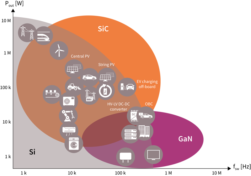
Figure 1. Suitability of Si, SiC, and GaN for power supply applications
Introduction
Silicon power devices, such as MOSFETs and IGBTs, have a long history of reliable operation in power applications. They are low-cost, with a proven track record, and there’s a wide choice of suppliers so that designers can have a second source. They are also a familiar, well-established option, with power engineers having a long experience working with them.
While that makes silicon suitable for many uses, more recently, the attention of most design engineers has switched to wide bandgap devices (WBG), typically SiC or GaN. They offer increased switching frequencies, higher efficiency, and greater power density than silicon, so power supplies can be smaller and lighter, or the output power in a given form factor can be greater.
Figure 1 shows typical applications for Si, SiC, and GaN devices in power supplies.
Cost and efficiency considerations
WBG components are more expensive than silicon alternatives, but over their lifetime, they will save money due to their higher efficiency, thus reducing power consumption as well as minimizing the need for active cooling. There are also financial savings from lower shipping costs due to smaller power supplies.
There is, therefore, a trade-off to be considered for each application as to whether savings in the total cost of ownership (TCO) with WBG devices are enough to justify their higher purchase price compared to silicon alternatives. This calculation needs to be explored for each use case, as it depends on multiple factors, including the voltage needed, the space available for the power supply, and cooling requirements.
For example, in a data center, improved efficiency in the power supply means lower electricity usage and less cooling required – which are major considerations in the overall running costs. In one customer project Infineon worked on, the efficiency of the power supply increased from 97 to 97.8 percent due to switching from silicon to WBG. This meant there was a payback period of three years, while the lifetime of the power supply is six to seven years – so moving to WBG was a clear winner.
Wide bandgap in practice
Ultra-compact 240 W charger
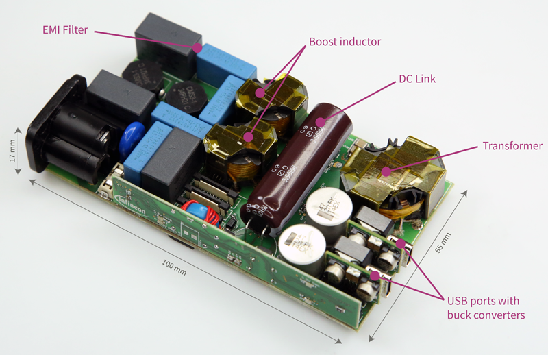
Let’s look in more detail at an example application: an ultra-compact charger for a portable consumer device (see Figure 2) with two USB ports.
Recent environmental legislation, particularly in the European Union, requires that universal USB-C chargers be developed for consumer devices to reduce waste. These chargers must be able to deliver high enough power to charge multiple devices simultaneously. They must provide a range of output voltages, from 5 V up to the 48 V maximum voltage specified by the USB-PD (power delivery) standard. They also need to be able to operate from different AC main supplies around the world, ranging from 90 VRMS to 265 VRMS.
USB-C cables are rated at 5 A, so with output voltages up to 48 V the universal charger must be able to deliver up to 240 W. This is much higher than the 65 W output power achieved by today’s USB chargers.
Click image to enlarge
Figure 2.Ultra-compact charger
The thermal aspects of the converter design are critical, with only passive convection radiation and convection available to dissipate heat. With WBG components enabling higher power density and thus a smaller converter, we need to ensure that the surface temperature does not exceed a suitable maximum temperature – typically stated as 70ºC.
To meet these requirements, we need a converter design based on a three-stage approach to handle the wide input and output voltage ranges. To minimize the size of passive components and thus enable a compact design, we need to employ very high switching frequencies.
It is suitable to use a three-stage approach with two interleaved totem-pole stages for the PFC stage, a DCX stage (DC transformer) running continuously at its resonance frequency, and two subsequent buck stages (see Figure 3).

Click image to enlarge
Figure 3. Topology of the ultra-compact charger [1]
This design uses CoolGaN™ integrated power stages (IPS) with Infineon’s CoolGaN™ gate injection transistor (GIT) technology, which is based on a hybrid-drain high electron mobility transistor (HEMT) with a p-GaN gate. The GIT HEMTs are used in a half-bridge configuration, with matching drivers in all HV sockets and CoolGaN™ Schottky Gate (SG) HEMTs 100 V[1] in the buck stage.
The entire system can deliver the required 240 W with two independent USB-C outputs and achieves an excellent power density of 42 W/inch3 – much higher than the figures of 16 W/inch3 to 20 W/inch3 achieved by a typical phone charger today.
Power supplies for data centers
Another important application for power supplies, as mentioned earlier, is the data centers. The processing power in data centers worldwide is growing rapidly, partly due to cloud services, artificial intelligence (AI), and cryptocurrencies. In these data centers, there is a trend toward investing in high-efficiency power supplies for servers to reduce costs by cutting electricity consumption.
A typical high-efficiency power supply for servers is comprised of a bridgeless PFC stage such as a totem-pole stage and a resonant DC-DC stage such as an LLC converter. For 12 V output systems, a center-tapped transformer is often used, while for 48 V output, a full-bridge rectification is a good option.
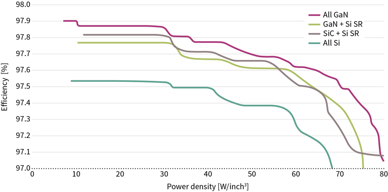
Figure 4 compares the efficiency and power density for different server power supplies delivering 7 kW with a 54 V output. It can be seen that an all-GaN design performs best, both in terms of efficiency and power density that can be achieved.
Click image to enlarge
Figure 4. Pareto optimization results for high power server power supplies, showing efficiency vs. power density [2]
High power, ultra-compact DC-DC server power supply
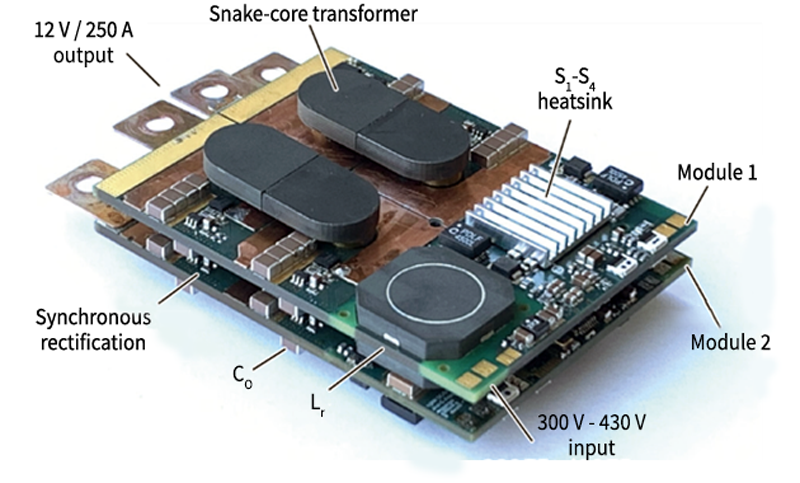
Another example power supply module for data centers is shown in Figure 5. One board measures 89.5 mm × 66.0 mm × 13.5 mm. It delivers 1.5 kW and achieves a power density above 300 W/inch3. At 10 percent load, the efficiency is 92.3 percent, while at 50 percent load, efficiency reaches 96.7 percent.
Click image to enlarge
Figure 5.Ultra-compact DC-DC power supply module for data centers [3]
In fact, Figure 5 shows two modules combined in an input-parallel output-parallel (IPOP) configuration sharing one transformer core. In this configuration, the modules can deliver 3 kW output power at 12 V and 250 A output current, with a power density of 345 W/inch3.
The snake-core transformer used in this module enables ideal current sharing between the phases and modules, with reduced core losses due to its single flux path and shared transformer core between the two modules.
Conclusion
Today’s power supply applications often demand excellent efficiency and very high power density, plus the ability to handle broad input and output voltage ranges.
While WBG semiconductors, such as GaN and SiC, have a higher up-front component cost than silicon devices, they typically enable lower total system costs over their lifetime due to factors including reduced power dissipation and more compact size.
For any particular application, it is worth evaluating the benefits offered by WBG devices, both technically and in terms of the total cost of ownership, as demonstrated in several applications throughout this article.
Visit our WBG technology page to discover more about Infineon’s broad portfolio of wide-bandgap products and solutions designed to meet the efficiency and power density requirements of modern high-power applications.
10-12 May 2022: Join us at PCIM Europe in Nuremberg in Hall 7 or digitally
This year, we’re pleased to have again the opportunity to present our Si and WBG power solutions to you in person and digital. Our hybrid concept will give you maximum flexibility for your trade show experience. Infineon will present the latest trends in power semiconductors and wide-bandgap technologies at 20 demo stations – clustered to your application of interest. Join us!
References
[1] Dr. Matthias J. Kasper, Dr. Jon Azurza, and Dr. Gerald Deboy, “GaN Integration Enables Next-Generation USB-C Chargers with Ultra-High Power Density and Wide Output Voltage Range,” in Applied Power Electronics Conference (APEC), 2022.
[2] J. W. Kolar, J. Biela, and J. Miniboeck, “Exploring the Pareto Front of Multi-Objective Single-Phase PFC Rectifier Design Optimization - 99.2% Efficiency vs. 7kW/dm3 Power Density,” in Proc. of the 6th Int. IEEE Power Electronics and Motion Control Conference (IPEMC), pp. 1–21, 2009.
[3] Knabben,G.C.;Zulauf,G.; Schäfer, J.; Kolar, J.W.; Kasper, M.; Azurza Anderson, J.; Deboy, G. “Conceptualization and Analysis of a Next-Generation Ultra-Compact 1.5-kW PCB-Integrated Wide-Input-Voltage-Range 12V-Output Industrial DC/DC Converter Module.” Electronics 2021, 10,2158. https://doi.org/10.3390/electronics10172158

.jpeg)