Smart strategies can avoid adverse, and often unforeseen, effects on RF emissions and end-product compatibility
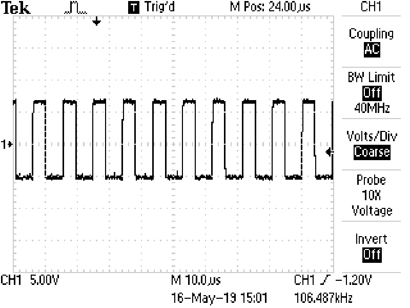
Figure 1: The Vg waveform under relatively heavy, resistive loading. (f=100kHz)
In response to ever evolving power supply efficiency standards, power supply manufacturers are using burst-mode operation (amongst a sea of other energy saving strategies) to decrease the standby power consumption of external power adaptors. Efficient conversion techniques do not come without some cost. Burst-mode operation can have adverse, and often unforeseen effects on RF emissions and on end-product compatibility. This article will provide a brief overview of the potential issues and some possible solutions.
When the Department of Energy (DoE) put its now familiar Level VI efficiency requirements into place in 2016, electronic equipment manufacturers around the globe needed to react – adopting new strategies designed to meet stringent new requirements for average-active-mode efficiency and for quiescent power consumption. Now, as Code of Conduct (CoC) Tier 2 legislation nears adoption in the European Union, a similar industry trend is taking hold. The new legislation will require no-load input power for some external adaptors to stay below a mere 75mW, and will also specify a challenging efficiency target for operation at 10% of rated load. Meeting either of these mandates is no small feat for a power supply, and utilization of burst-mode operation will continue to prove essential in designs going forward.
Burst-mode is an operational mode whereby the power supply control circuit and switching circuit (and sometimes additional features) are intermittently disabled when the direct current (DC) load is particularly light, or absent. The feature can be thought of as a gating signal with a duty cycle that is proportional to the load superimposed upon the standard pulse-width modulation (PWM) switching signal, which itself is essentially a pulse train with an on-time that is proportional to the instantaneous DC load. The burst-mode “gating signal” simply has a much longer period, such that several of the PWM pulses occur during a single “burst.” Relatively speaking, a lot of energy is lost when a metal-oxide semiconductor field-effect transistor (MOSFET) switches states, which happens during every cycle of standard switch-mode power supply (SMPS) operation. These losses per unit time are proportional to the switching frequency (because the switch changes states more frequently per unit time). If the DC load is light, and not much energy needs to be transferred from primary to secondary, the PWM duty cycle will decrease to some minimum value but would otherwise still be changing states just as often, assuming a fixed frequency device.
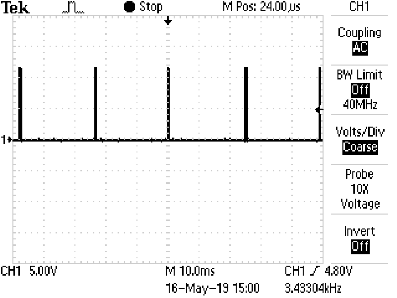
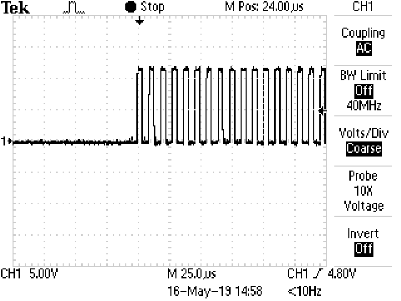
Since changing the duty cycle of the PWM signal does not necessarily effect efficiency, the idea of the additional gating signal is to completely eliminate switching cycles that are not needed to hold up the load, effectively reducing switching losses. This is an important practice, not just for no-load operation (reducing quiescent consumption), but also for light-load operation because the dominance of any loss mechanism is markedly greater when the output power is small. To exemplify this operational mode, Figure 1 shows the MOSFET gate pulse signal (Vg) of a representative power supply while operating under a heavy resistive load (a regular, periodic pulse train with fixed period and fixed duty cycle), while Figure 2shows Vg while the power supply is operating under no-load. Figure 3shows a zoomed-in view of the “bursts” shown in Figure 2. Notice that original pulse train has not changed frequency, but rather entire segments of the pulse train have been gated out, eliminating a multitude of MOSFET transitions.
Click image to enlarge
Figure 2: A Vg pulse train being gated by burst-mode. The individual PWM pulses are not visible due to time scale (see figure 3 for a close up)
Click image to enlarge
Figure 3: A zoomed in view of one “burst” beginning. PWM pulse train frequency is largely unchanged
Although burst-mode operation is an innovative approach to reducing no-load and light-load losses, there are still a number of design implications to consider. Here are two cases in which we have seen application compatibility issues that trace back to burst-mode operation.
Case 1: Excessive DC Voltage Fluctuation
In one customer scenario, several power supply units (PSUs) had failed out of part of their incoming inspection process. The customer’s equipment would not start up when power was applied by some of the converters. However, their program was in production for some time, and they were placing regular orders without any reported issues. The manufacturer was eager to see why some small subset of units were not passing.
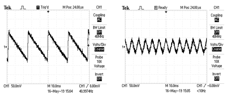
The customer returned several units for evaluation. When the manufacturer received the returned units, they quickly discovered a potential issue: although the output voltage may have appeared steady when measured with a digital voltmeter, oscilloscope scans showed that the output voltage was rapidly fluctuating by as much as 5% of the rated DC level when the power supplies were unloaded or lightly loaded. This is a reasonably common artifact of burst-mode operation, as the secondary side of the converter is receiving its energy in discrete and separated chunks. The degree of fluctuation was not very consistent across all sampled units, likely due to tolerances within the control integrated circuit (IC). Through discussions with the customer, the PSU manufacturer learned that end device idle load was very light, and that there was an under-voltage lockout circuit in the system that would prevent it from turning on with a low, or in this case, overly noisy input voltage. To exemplify representative waveforms, Figure 4shows an AC coupled comparison of the DC output of a converter operating in burst-mode, versus normal operating mode. Notice that the peaks of the sawtooth waveform are concurrent with the energy bursts shown in Figure 2.
Click image to enlarge
Figure 4: DC output during burst-mode operation (left) and during normal operation (right)
While the output voltage was still remaining within manufacturers +/−5% specification, the waveform associated with the burst-mode operation triggered the equipment to enter an under-voltage-lockout condition and remain latched off. To resolve the issue, the manufacturer was able to adjust the PSUs burst-mode activation setpoint to be just below the equipment’s worst-case quiescent load. As a result, the customer did not have to make any changes to their equipment, while still managing to meet the no-load power consumption requirements associated with DoE Level VI.
Case 2: RF emissions
In another instance, a customer was upgrading to a new Level VI-compliant power supply during a product redesign. Of course, the new system needed to be re-evaluated against the current safety and electromagnetic compatibility (EMC) standards for information technology equipment (ITE). When the EMC test lab was evaluating the system for electromagnetic compatibility, they found that the system exceeded emissions limits while idling, but passed during normal system operation. This spawned a bit of a conundrum as power supplies will typically exhibit the greatest emissions at full load. Further evaluation, however, revealed that the customer’s idle load was so low that the power supply was still operating in burst-mode. As a result of the converters resonant topology, the PSU emissions were extremely low during normal operation, and actually higher at light-load.
Although the power supply did pass emissions testing at light-load on its own, the pass margin was within a few dB. The combination of the power supply emissions and equipment emissions under these conditions was enough to cause a system-level failure. A review of the control ICs burst-mode operation revealed the root of the issue.
For this particular control chip operating in burst-mode, the switching frequency was actually modulated over a large range and was not fixed. Fixed frequency operation was restored under heavier-loads. The light-load switching frequencies were not as effectively attenuated by the converters EMC filters, which had been designed for the normal operating frequency. Additionally, though not the case in this particular situation, burst-mode operation of higher-power converters is also frequently accompanied by a shutdown of any active power factor correction (PFC) circuitry, as 61000 series harmonic current regulations are not applicable to light-load operating conditions. This shut down contributes to the release of harmonic content onto the mains and also possibly onto external radiators (cables) that would otherwise be mitigated by the active PFC. In a similar fashion to first example scenario, the manufacturer was able to adjust the burst-mode setpoint to a suitable level for the application and still keep the no-load power consumption within limits.
With the ever-increasing use of power conversion products in households and offices worldwide, efficiency mandates and the technological advances that make them possible are absolutely essential. However, it is important to consider the ramifications of those efficiency-boosting measures. In both of the cases outlined in this article, the solution was relatively simple and required very little redesign. Going forward, as efficiency requirements grow ever-more stringent, and power supply technologies become more complex, additional measures will need to be considered to mitigate the side effects brought on by these new technologies.
TT Electronics