Silicon Class D amplifiers have been prevalent in audio applications for 70 years, but are now reaching their performance limits. Can GaN offer an alternative?
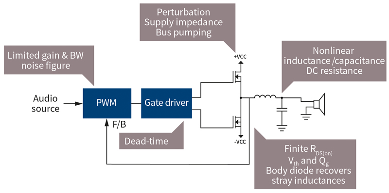
Figure 1: Basic block diagram of a Class D amplifier design
Audio is a complex application space, especially when operating in the realms of the audiophile. The highest-end audio equipment comes with a hefty price tag and audio amplifiers of differing types attract followings of users who believe their choice best reproduces a true interpretation of the original recording being played. While the merits and weaknesses of various classes of amplifier design are bounced back and forth in various audiophile forums, there are plenty of application spaces where energy efficiency also plays an important role.
Class D amplifiers were first suggested in the 1950s (figure 1). The alternatives, Class A, AB and B, all use transistors in their linear regions to replicate an amplified version of the input signal as accurately as possible, but such designs have a theoretical efficiency limit of below 80% and, in practice, lie at 65% or below. With Class D designs it was proposed that the incoming signal would be used to control a push/pull pair of switching devices with pulse-width modulation (PWM), allowing them to operate in either on or off mode. As a result, they would not be operating in their linear region making the design capable of delivering a theoretical 100% efficiency together with zero distortion.
At the time, there were no devices available that could realise the full potential of Class D, until silicon MOSFETs with suitable device parameters became available. Since then the Class D amplifier has seen much success, especially in battery-powered devices such as smartphones, hearing aids and Bluetooth headsets where the high efficiency and low heat dissipation is very advantageous. Of course, higher power amplifiers, such as for televisions and in automotive, have also benefitted from this technology, making for compact designs with little to no heatsink requirement.
Most recently the technical specifications of GaN-based high-electron-mobility transistors (HEMT) have opened the door to even better Class D amplifier performance.
A new switching technology to match the demands of Class D
The ability of a Class D amplifier to deliver high efficiency and low distortion lie with the switching devices chosen. Firstly, the on-resistance needs to be as low as possible to reduce I2R losses. Secondly, the switching losses need to be minimal in order to support higher switching frequencies. The efficiency of all classes of amplifiers typically tends to be poor at the lowest power outputs due to losses in the power devices. Only once a certain power output is attained does the efficiency start to improve.
Class D amplifiers can implement a so-called multilevel technique where the maximum output voltage is limited when outputting audio at lower volumes, a method that helps to improve efficiency at low power outputs. As the audio moves to the higher output levels, the full voltage swing is made available to the switching devices. At the lower output levels, zero-voltage switching (ZVS) is employed while at higher output levels the amplifier operates a hard-switching approach. These two modes of operation impact the losses that result from the switching.
In ZVS operation mode, the transition of the output is achieved by an inductor current commutation. As a result, any switching losses, and resulting power loss, in the switching device are eliminated. However, to avoid shoot-through across the two devices, a small blanking delay has to be inserted to ensure that the off-state of the previous switching cycle has been attained before the on-state of the next switching cycle is engaged. This changes the output waveform from that intended by the PWM output leading to distortion of the audio signal. The blanking time is determined by the output capacitance, Coss, of the power devices used. Compared to Si MOSFETs, GaN transistors have a significantly lower Coss meaning the blanking time can be kept to a minimum, which minimises distortion.
Hard switching at higher power outputs implies a non-zero voltage at the output when the power device is switched on or off. An Si MOSFET has a body diode in which a reverse-recovery charge (Qrr) builds up after the switch is turned off. This needs to be discharged, and the time for this factored in, before the opposing switch enters its on-state. GaN transistors differ here significantly since there is no inherent body diode and therefore no Qrr. This results in much cleaner switching waveforms, improved distortion figures, and higher overall efficiency.
Unfortunately, the challenges posed by Coss also need to be dealt with when using GaN. However, the energy stored is significantly lower than with Si MOSFETs, resulting in less energy being dissipated at the next turn-on cycle. As this contributes significantly to losses at higher frequencies, GaN demonstrates an especially beneficial improvement over Si. On top of this, the move to GaN also offers a much lower on-resistance in a smaller die size, enabling engineers to design more dense, compact audio solutions in addition to delivering better audio quality.
How the GaN benefits manifest themselves in their design
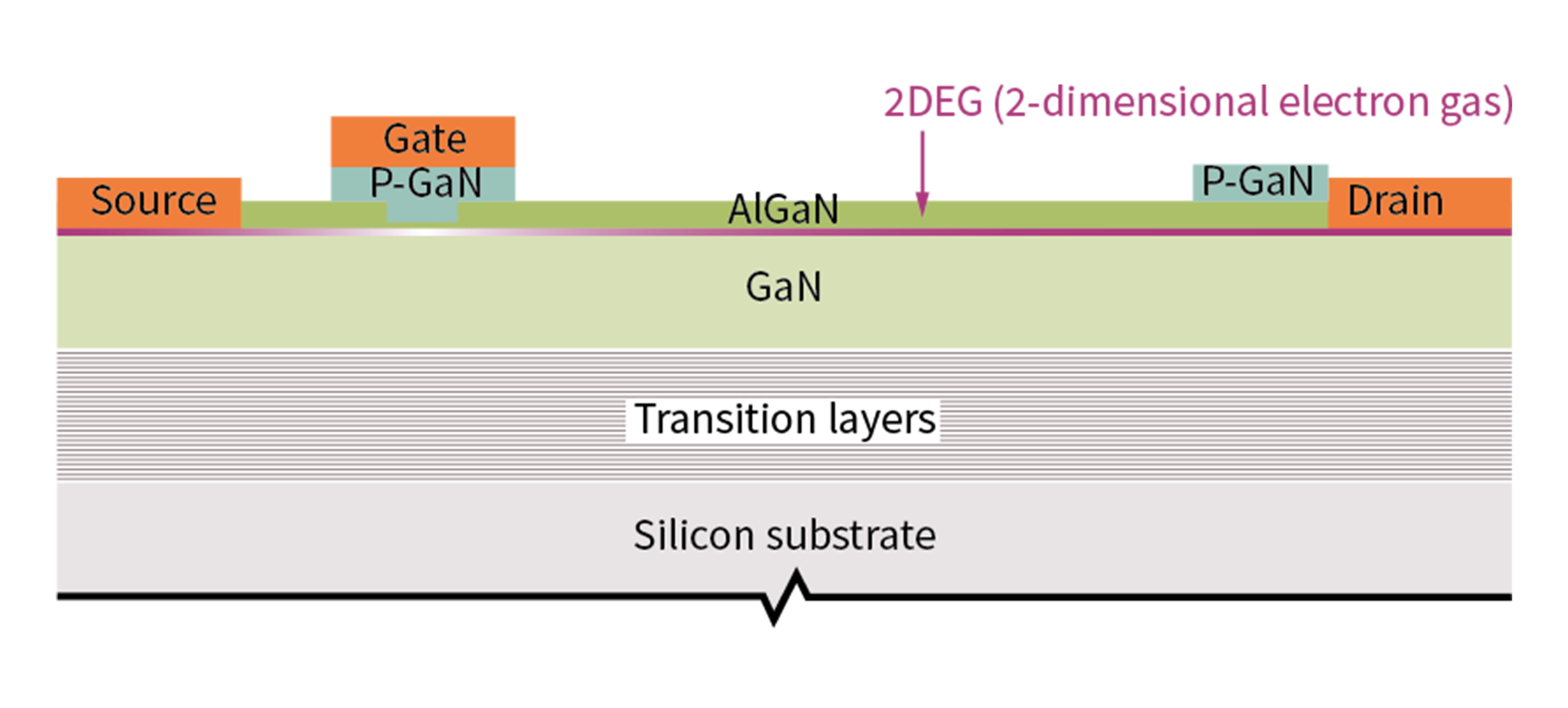
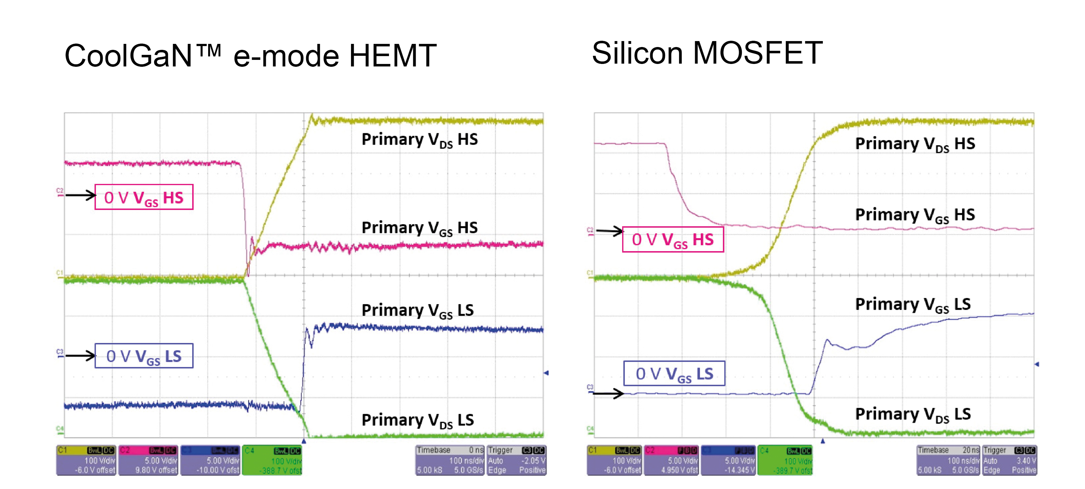
Like their silicon counterparts, GaN HEMT devices have a gate, drain and source terminal. A two-dimensional electron gas (2DEG) layer provides a pool of electrons that implement a short circuit between the source and drain with a very low resistance. The p-GaN gate stops conduction when there is no gate bias applied (VGS = 0 V). It should be noted that GaN HEMTs differ from Si MOSFETs in that they are bi-directional and will allow reverse current flow should the drain voltage become lower than the source voltage. The absence of a body diode eliminates much of the switching noise associated with the PN junction common to Si MOSFETs, thus providing the much cleaner switching for which they are noted (figure 2).
Click image to enlarge
Figures 2a & 2b: The structure of a GaN HEMT transistor (2a) and the superior switching characteristics that benefit Class D amplifiers compared to Si MOSFETs (2b)
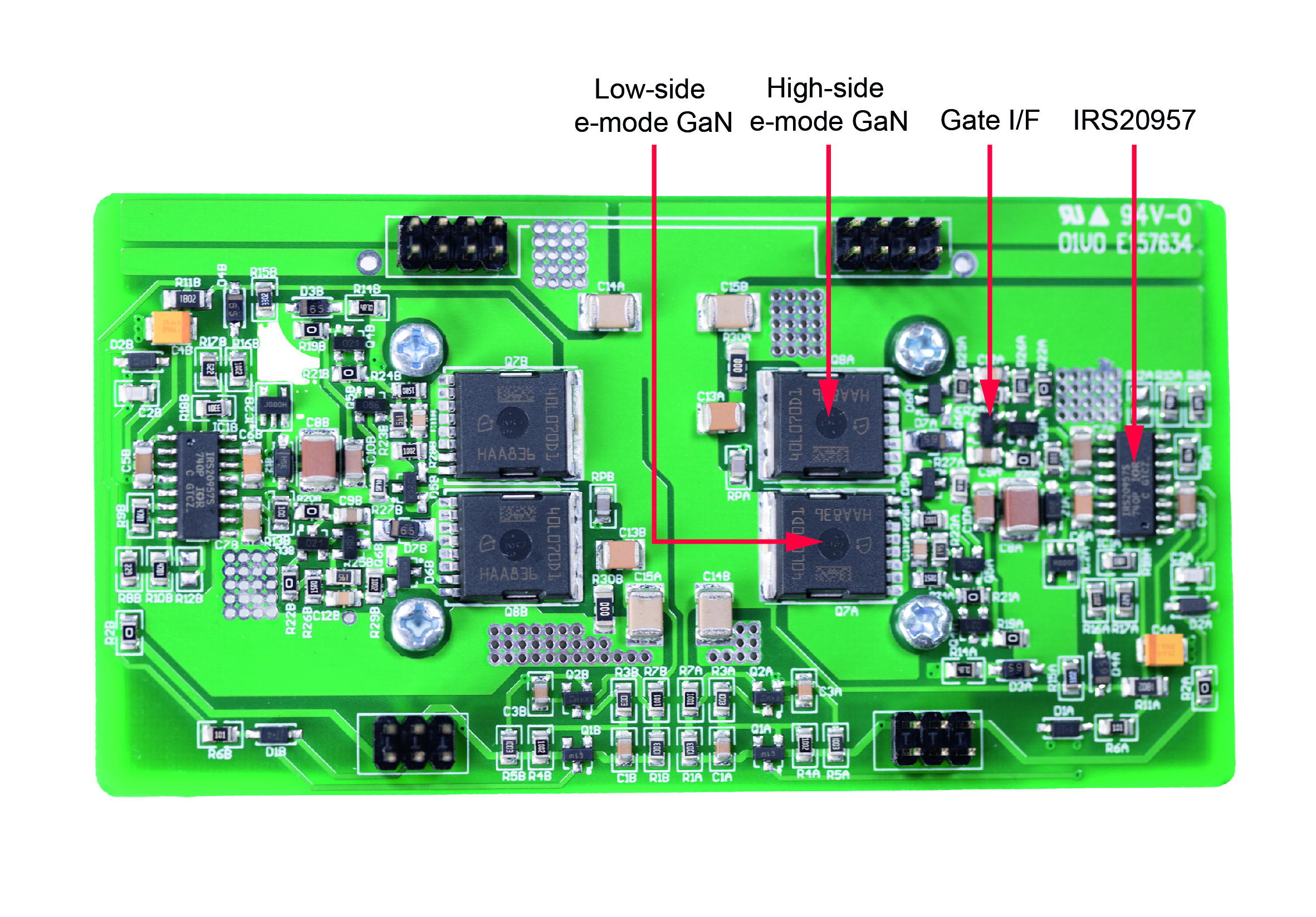
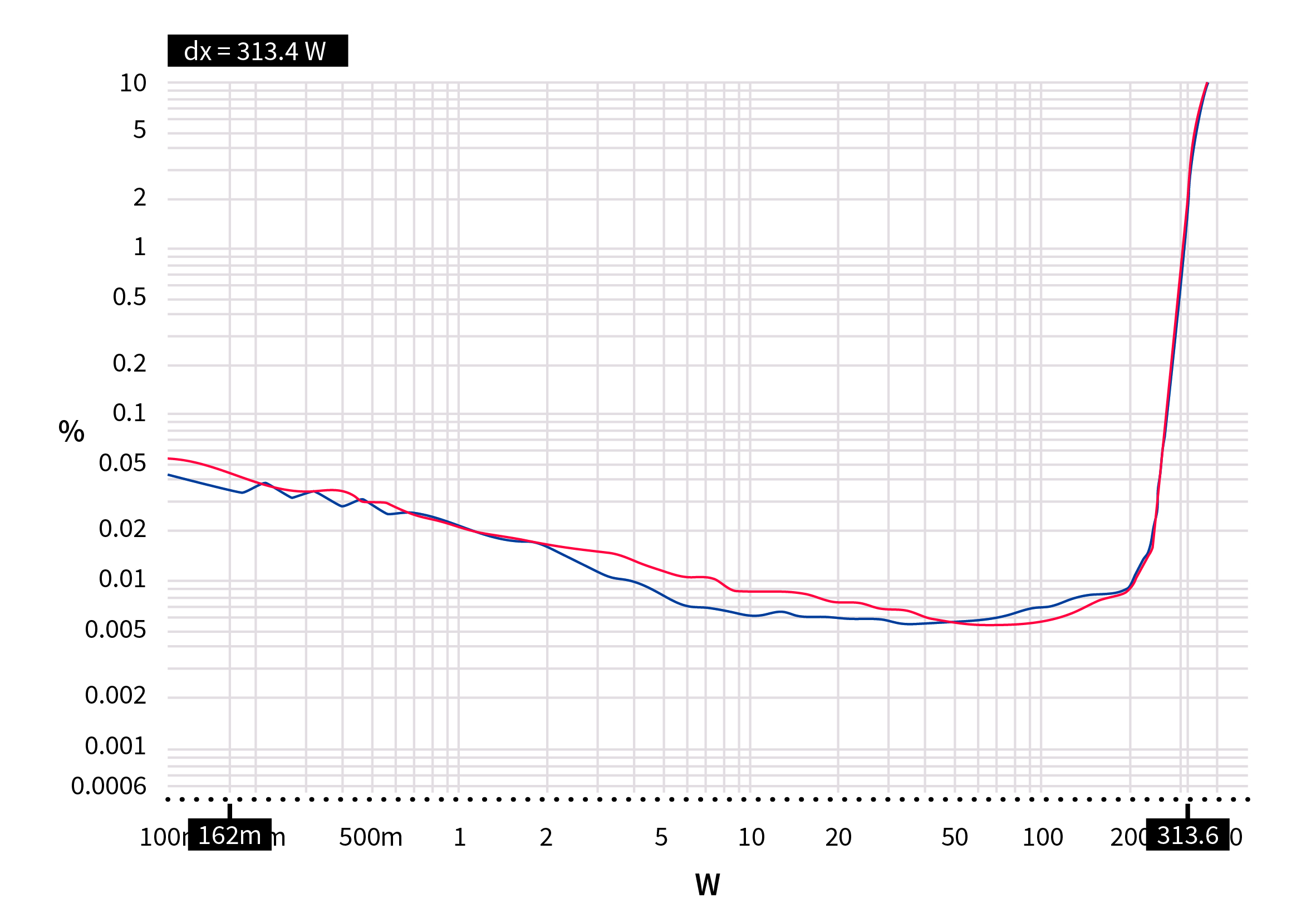
Implemented in a 250 W Class D design, a device such as the IGT40R070D1 E8220 that provides a 70 mΩ RDS(on)(max) together with a 200 V Class D driver IC (IRS20957S) can deliver 160 W of power in to an 8 Ω load without the need for a heatsink (figure 3). At 100 W, the THD+N is a respectable 0.008%. With switching set at 500 kHz, the THD+N measurements show no discernible change in distortion in the region where the amplifier moves from ZVS to hard-switching, which occurs at a few watts, and the hard-switching region is very clean and quiet.
Click image to enlarge
Figures 3a & 3b: The 250 W Class D amplifier design (3a) and the THD+N measurement (3b)
Summary
The introduction of the Class D amplifier concept seventy years ago offered an unheard-of, but at the time theoretical, audio fidelity and superb efficiency. While traditional silicon MOSFETs have improved in their characteristics and have continuously shown advancement in their design, the impact of both Qrr and Coss limit the upper switching frequency, impact on efficiency, and ultimately result in unwanted audio distortion in Class D designs. The larger die size needed to attain lower RDS(on) also means that more efficient designs require more volume. With the availability of GaN transistors, the elimination of Qrr and the large reduction in Coss ensures that higher switching frequencies can be used while delivering superlative THD+N results. The inherent low RDS(on)(max) in a small package ensures that Class D GaN-based amplifiers can provide high audio fidelity in a small volume and without the need for bulky and heavy heat-dissipation solutions.