Dynamic voltage control strategies hold the key to power savings.
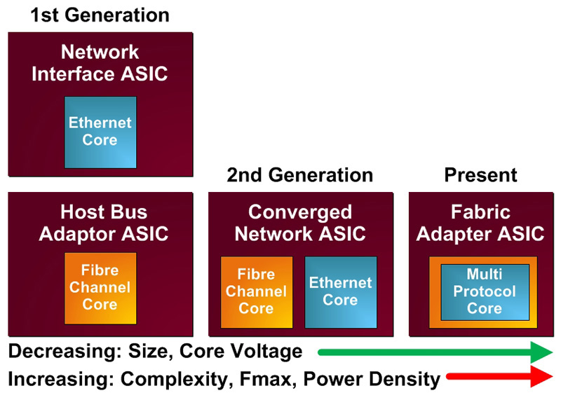
Figure 1: Development of CNA ASICs
For some designs, reducing circuit-board power dissipation by 25% to 30% would just be a nice outcome. For other designs, it's an absolute necessity. Designers of products using the latest high-performance integrated circuits must carefully manage circuit-board power dissipation because one can describe new ASICs, SoCs (systems on chip), and processors in only one way: They are hot! What led to this problem is increasing power density in IC technologies. Even with shrinking transistor sizes and lower operating voltages, the number of transistors on a chip and the frequency at which they switch have been increasing at even greater rates. The result is more power dissipation in smaller areas that ever before. Converged network-adapter evolution In the CNA (converged network-adaptor) market, ASICs combine the functionality of a NIC (network-interface card) with an Ethernet-processing core and an HBA (host-bus adapter) using Fiber-Channel processing cores. The development of these highly adapted ASICs traces from separate functional ICs to devices with multiple core types on a single SoC. The evolution continued to the present-day Fabric-Adapter ASIC capable of handling multiple protocols natively through a single IC core (Figure 1). This feat is possible thanks to smaller IC-fabrication-process nodes and higher transistor counts than ever before possible. Multiple and lower operating voltages, along with higher clock switching speeds, facilitate this processing power in a smaller footprint than previously possible. While this advancement is exciting, there are limits to any technology, including these powerful new ASICs. Board designers who use these ICs now have more challenges than ever to deal with. On small, compact boards, the design challenges that higher power densities create include:
- High local IC temperatures, which are near or at specified maximums
- The need for heat sinks or other heat-mitigation measures
- Increased operating temperatures of adjacent devices
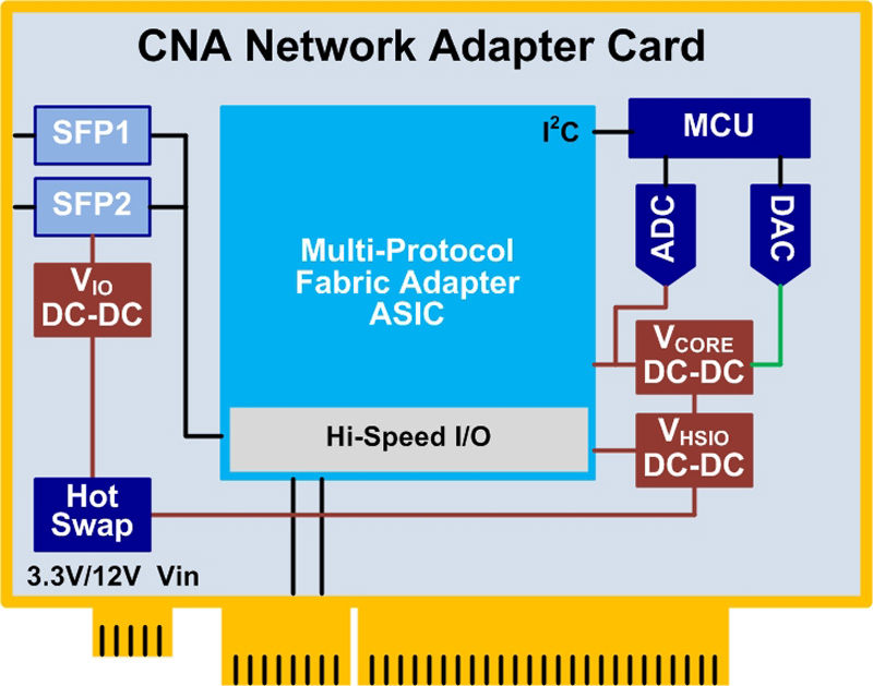
Power-management strategy through voltage-supply scaling Using the example of the CNA card, a new technique for reducing power dissipation is to lower the ASIC core's operating voltage(s) while maintaining manufacturer-specified operating conditions. The savings can be significant, as power dissipation is primarily a function of the square of the device's operating voltage. When load and digital processing conditions permit, reducing the ASIC's Vcore can yield power savings of 30% or more per IC. Those conditions include I/O loading, clock speed, and other parameters such as temperature and operational characteristics. At appropriate times, a circuit controlling the ASIC's Vcore can change the Vout of the supply delivering that voltage. In Figure 2, a dedicated MCU communicates with the ASIC and, by implementing a closed-loop trimming algorithm, adjusts the Vcore DC-DC converter in real time. The MCU measures Vcore from the DC-DC and then sends digital correction signals to the DC-DC by means of a voltage it generates with an external DAC. Challenges of traditional voltage-scaling methods One of the challenges of implementing a method for setting the Vcore power supply to multiple values is the need for multiple external components in a closed-loop-control configuration. The measurement of the power supply's output voltage is subject to the accumulation of errors due to ground potential variations and single-ended voltage-measurement techniques. Another disadvantage of single-ended measurement is that it's not immune to noise. Traditional single-ended measurement is a poor alternative to differential input sensing and results in accuracies no better than 1.5% error (min). Other MCU-based implementation challenges include the need for an external watchdog timer to ensure that a hung-processor condition does not occur. Finally, a custom-built implementation is the most expensive alternative, especially when it requires a large number of discrete ICs. Another item often overlooked is the risk and complexity of the stable closed-loop trimming algorithm itself. A hung MCU or over-ranged ADC or DAC condition can result in unpredictable operation. Being too conservative and missing specification values will reduce power savings.
A complete power-management implementation In addition to accurately scaling Vcore for multiple operating values, a complete board-management implementation should offer all of the following features:
- Voltage monitoring (all supplies)
- Power supply sequencing
- PCIe requirements for hot swap of 3.3V and 12V
- Power feed control to SFPs
- Reset-Tree generation
- I2C link for multiple-purpose communications


