Combining Lowest RDS(on) + SMT for Space-Limited, High-Performance Apps
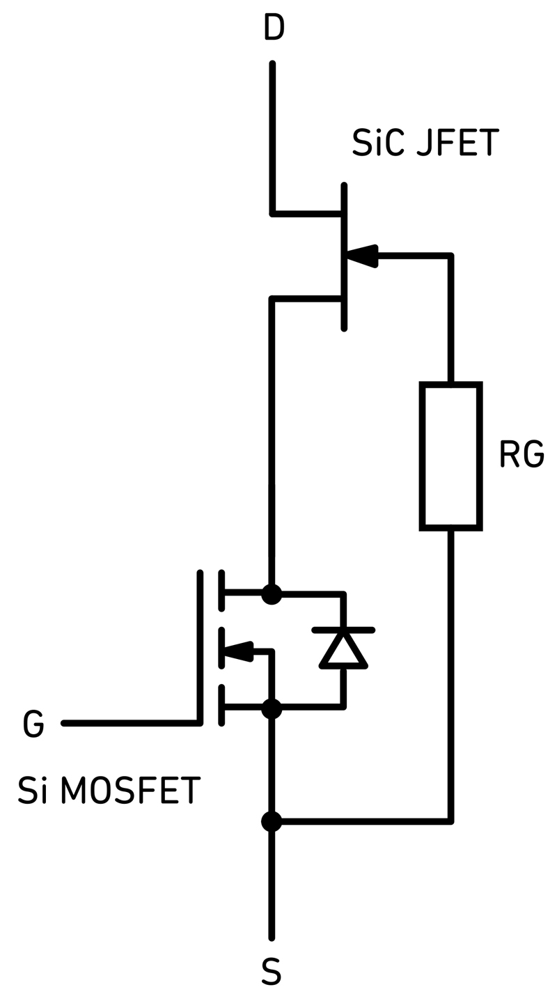
SiC FETs combining a Si-MOSFET and SiC JFET in a cascode bring the performance advantages
Figure 1: The Qorvo SiC FET – a ‘cascode’ of a Si-MOSFET and SiC JFET
The performance of wide band-gap (WBG) semiconductor switches such as silicon carbide cascode FETs (‘SiC FET’ henceforth) (Figure 1) and SiC MOSFETs is closely tied to its package. At the pure technology level, nanosecond switching speed and low specific on-resistance result in very low losses, allowing much higher current levels to be handled versus silicon for the same die size. However, thermal resistance to the outside world practically limits junction temperature in a real power-conversion circuit, and any lead inductance affects attainable switching speed, so device manufacturers offer different packages that give the optimum performance depending on the application requirements.
Different packages suit different applications
Why does the optimum package for a SiC FET depend on the application? A traditional through-hole leaded package with a large tab, such as the TO-247 style, can be attractive, allowing backward compatibility in existing designs that use Si-MOSFETs or even IGBTs. Indeed, one of the significant advantages of the SiC cascode FET is its pin-compatibility and gate-drive similarity with these older technologies, which enable an easy upgrade with just minor circuit component changes for a significant efficiency or power-rating boost.
The large pad area of a TO-247 device is also great for direct attachment to a heatsink for tens of watts of dissipation with low junction temperature rise. However, downsides of the package are significant size, labor cost of the mechanical assembly, and lead inductance and resistance. As a result, particularly in high-power density designs, a surface mount technology (SMT) package is usually preferred, which can be automatically placed and reflow-soldered. Resistance and inductance in the connections to the PCB are also minimized, close to zero. However, heat extraction can be less efficient, with a thermal route normally through the electrical terminations into the PCB. This can limit high-power operation, which is where the advantages of WBG devices are supposed to be seen.
Putting values to the package limitations
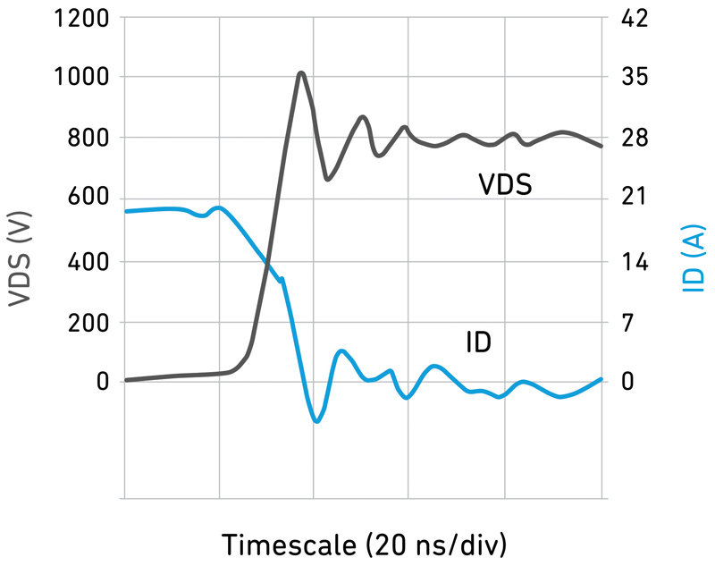
The inductance and stray capacitance of PCB traces and package leads cause transient voltages and currents to be generated from the fast voltage and current edge rates of WBG devices. SiC for example, is capable of more than 100 kV/µs and 1000 A/µs (Figure 2), and this contributes to low switching losses, especially in ‘hard switched’ power-conversion topologies.
However, just 10 nH or about 10 mm of lead length produces a 10V spike from this current edge rate, from the familiar V = -L di/dt. If this lead is the source connection and is common to the gate drive loop, 10V is injected into the gate circuit which leads to higher power losses due to gate de-bias and poor noise-immunity. Similarly, just 10 pF of stray capacitance with 100 kV/µs edge rate results in 1 amp displacement current from I = C dV/dt, with an indeterminate return path that might include sensitive signal connections. The capacitance also rings with the stray inductance to potentially produce circuit instabilities and undesirable EMI signatures.
Click image to enlarge
Figure 2: Example edge rates from a circuit using a Qorvo SiC FET
The effects can be mitigated, for example, by using a Kelvin connection to the source for the gate drive loop, using a negative off-state voltage and minimizing capacitances and inductances from careful layout practice. However, residual stray values can still be problematic with leaded packages such as TO-247, so edge rates are commonly deliberately slowed by tailoring the gate drive or by using snubbers, but at the expense of increased switching losses.
A lead-less package such as the PDFN type (power dual flatpack no-lead) largely solves the stray inductance issue and is offered by some WBG device manufacturers, with an emphasis on its smaller size footprint and low profile/thickness for high-density designs. Compared with a TO-247 leaded device, thermal resistance from junction to case (Rθ(J-C)) of the PDFN package is more than 10x worse due to insufficient heat-spreading, thus limiting its application at high power. Thermo-mechanical performance also suffers since there are no lead connections between the device and PCB to absorb stress resulting from thermal expansion mismatches.
As an alternative, the D2PAK package is sometimes offered for WBG devices and is available in 7-lead versions for high current handling, with a Kelvin connection for the source as an option. This surface-mount package still has ‘leads’ however, with resistance and inductance, and its Rθ(J-C) is 3x worse than the best TO-247 value. It does have the advantage of inherent wide physical spacing between the drain and other connections, allowing it to meet recommended creepage and clearance distances for high voltages.
TOLL packages are a good solution
It is possible to use a TOLL package (TO-leadless, MO-229), Figure 3 and approach the ideal with Rθ(J-C) as low as 0.1°C/W. An example device is the UJ4SC075005L8S from the Qorvo SiC FET range. This low value is achieved by advanced cell design, silver sintering die-attach and wafer thinning. The TOLL package is 30% smaller in footprint than the D2PAK with a size of 10mm x 11.7mm. There is a large space between the drain and other connections but, with much shorter leads than D2PAK, much lower parasitic inductance results. Also, at 2.3 mm the TOLL is half the height of D2PAK, which affords additional fin height to the heatsink in the thermomechanical design, while adhering to the same overall form-factor in space-constrained designs such as server power supply units (PSU). This potentially further reduces device junction temperature compared with a D2PAK solution in the same application.

Click image to enlarge
Figure 3: The TOLL package now available for SiC FETs
In the TOLL package, all heat transfer is effectively through the source pins and drain pad connection, which can be re-flow soldered to a copper land on the mounting PCB to conduct heat away. The heat must still go somewhere, and a compact PCB-solderable SMT heatsink could be fitted on the back side of the PCB directly underneath, with vias making a thermal connection through the PCB. This thermomechanical design results in major savings in assembly costs, as the manual installation effort of a through-hole package and mechanically secured heatsink are completely eliminated, and both the FET and heatsink can be installed using automated assembly. The device could also be soldered to an insulated metal substrate (IMS) for the ultimate in performance and integrated with a mechanically attached heatsink that is bigger in size.
Top-side cooled SMT packages are also fast emerging in the market, offering even better performance. However, engineers will need time to overcome associated challenges of top-side cooled packages which include assembling multiple devices of different heights to the same cooling surface while also managing creepage and clearance requirements in the overall design.
Click image to enlarge
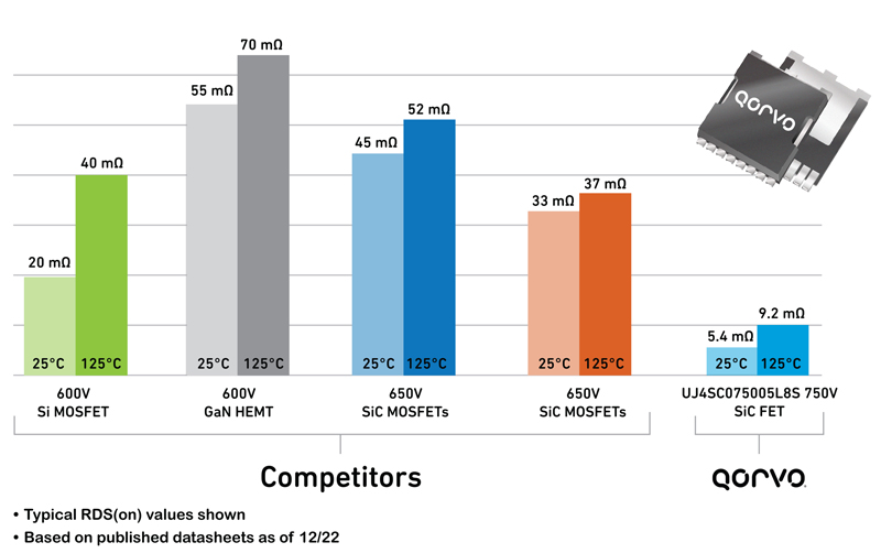
Figure 4: On-resistance achieved for different devices in TOLL packages in the same voltage class
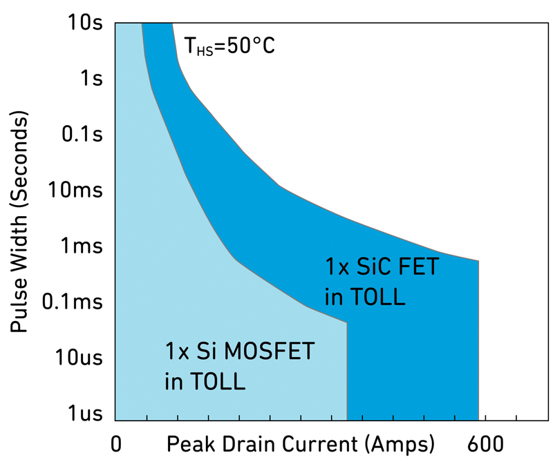
SiC FETs in TOLL packages achieve 10x peak current rating of Si-MOSFETs
In TOLL-packaged SiC FETS, the exceptionally low package thermal resistance, the low power loss due to ultra-low 5.4-milliohm on-resistance and high maximum SiC FET junction temperature of 175°C, all enable high peak current withstand capability and for longer time – the ‘I2t’ performance – compared with other switches. In power conversion circuits where loads can momentarily surge or go short, this provides a valuable extra safety margin in terms of the maximum peak current that the device can tolerate for a given pulse-width. When SiC FETs are used in a solid-state circuit breaker application, high transient fault currents are expected and must be withstood without stress. Figure 5 shows how a TOLL-packaged SiC FET withstands a given peak drain current for more than 10x the time of a Si-MOSFET before reaching a safe operating limit, improving robustness and allowing fault detection circuitry longer time to react, making it more immune to nuisance triggering with current spikes.
Click image to enlarge
Figure 5: Peak pulsed-current (I-t) current capability compared - SiC FET and Si-MOSFET in a Qorvo TOLL package
The applications
Cascode SiC FETs rated 750V available in the TOLL package from Qorvo showcase what is possible in a compact surface mount switch, optimized for low static and dynamic losses. As such, a family of these devices in various on-resistance ratings between 5-60 milliohms suits applications from several hundred watts to relatively high-power levels in the range of multiple kilowatts. This covers AC/DC power supplies, battery chargers, TVs and portable power stations as well as power conversion in alternative energy, datacomms and in industrial applications generally.
In circuit protection applications, SiC FETs in TOLL packages will find use in EV chargers, battery disconnection circuits and in building electrical smart panels, which are becoming more intelligent to offer dynamic load management. Because of the small size/high performance metric of Qorvo SiC FETs, they can be considered in end-uses where space is at a premium. In this situation, they could require less heatsinking and yield an overall lowered system cost along with higher power-density solution compared with using higher on-resistance devices from alternative technologies. This is even more the case when multiple alternative devices might need to be paralleled to achieve the same electrical and thermal performance as SiC FETs, incurring additional device costs and the overheads of handling and placement.
Conclusion
A wide band-gap semiconductor power switch is only as good as its package. Now that cascode SiC FETs are available in TOLL versions, their low loss can be leveraged to improve system power density even further.