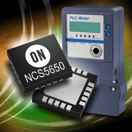
ON Semiconductor has introduced the NCS5650 - a new line driver device targeted at Power Line Carrier (PLC) communications applications such as smart metering, industrial control and street lighting. The NCS5650 is a high efficiency, Class AB, low distortion driver, specifically designed to drive power line mains and capable of accepting a signal from any power line carrier modem.
The NCS5650 contains an operational amplifier which can be configured as a unity gain follower buffer, or alternatively used to provide the first stage of a 4-pole low pass filter. The output stage has the capacity drive up to 2.0A peak into an isolation transformer or simple coil coupling to the mains. At an output current of 1.5A, the output voltage is guaranteed to swing within 1.0V or less on either rail, ensuring optimal signal-to-noise ratio (SNR) in harsh environments. The NCS5650 draws just 150μA while in shutdown mode. Power supply options are single-sided 6V to 12V and dual balanced �3.0V to �6.0V. With its unique full power bandwidth, the NCS5650 can operate in any region of the world while complying with local PLC frequency band regulations like CENELEC. "The advent of power line communications allows utility companies to add greater levels of functionality to their electricity distribution networks - thereby providing consumers more control over their energy consumption," said Simon Keeton, general manager of ON Semiconductor's Audio, Video and Interface products division. "When combined with an industry leading Spaced Frequency Shift Keying (SFSK) modem, like ON Semiconductor's AMIS-49587, the NCS5650 acts as an adaptive solution for PLC communications with a desirable balance of performance and price. Designs employing this solution will benefit from high levels of integration which provides a reduced component count and a decreased overall bill of materials." In addition, the NCS5650 offers a current limit programmable with a single resistor, R-Limit, together with a current limit flag. The device provides two independent thermal flags with hysteresis: a thermal warning flag to let the user know the internal junction temperature has reached a user programmable thermal warning threshold and a thermal error flag that indicates the internal junction temperature has exceeded 150°C. In shutdown mode the NCS5650 output goes into a high-impedance state.
 PDF
PDF