UD research team develops new way to make integrated photonics
The signals from a lighthouse to ships at sea is an early example of optical communication, the use of light to transmit information. Today, researchers in the field of integrated photonics are using optical communications principles to build high-tech devices, like lightning-fast computers, which utilize light instead of electricity.
At the University of Delaware, a research team led by Tingyi Gu, assistant professor of electrical and computer engineering, has designed an integrated photonics platform with a one-dimensional metalens -- a thin lens that can be designed at the nanoscale to focus light in a specific way -- and metasurfaces -- tiny surfaces made with nanostructures to manipulate the transmitted or reflected light-- that limit the loss of information. The team recently described their device in the journal Nature Communications.
"It's a new way to achieve integrated photonics compared to the conventional way," said doctoral student Zi Wang, the first author of the paper.
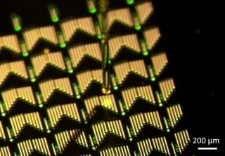
The team fabricated a tiny metalens on a silicon-based chip programmed with hundreds of tiny air slots, enabling parallel optical signal processing all within the tiny chip. They demonstrated high signal transmission with less than one decibel loss over a 200-nanometer bandwidth. When they layered three of their metasurfaces together, they demonstrated functionalities of Fourier transformation and differentiation -- important techniques in the physical sciences that break down functions into constituent parts.
"This is the first paper to use low-loss metasurfaces on the integrated photonics platform," said Gu. "Our structure is broadband and low loss, which is critical for energy efficient optical communications."
What's more, the new device developed at UD is much smaller and lighter than conventional devices of its type. It doesn't require the manual alignment of lenses, so it is more robust and scalable compared to the traditional free-space optics platforms, which require tremendous patience and time to set up.
This new device could have applications in imaging, sensing and quantum information processing, such as on-chip transformation optics, mathematical operations and spectrometers. With more development, this technology could also be useful in deep learning and neural network applications in computing.
"It's just much faster than conventional structures," said Gu. "There are still a lot of technical challenges when you try to actively control them, but this is a new platform we are starting with and working on."
Parts of the device were fabricated in the University of Delaware Nanofabrication Facility and at AIM Photonics in Rochester, New York.
While working on this project, Gu was inspired by conversations with fellow faculty members Dennis Prather, Engineering Alumni Professor of Electrical and Computer Engineering; Gonzalo Arce, Charles Black Evans Professor of Electrical and Computer Engineering; and Kenneth Barner, Charles Black Evans Professor of Electrical and Computer Engineering.
EurekAlert!, the online, global news service operated by AAAS, the science society: https://www.eurekalert.org/pub_releases/2019-09/uod-cat092619.php