There are many factors to consider when selecting an emerging technology
Figure 1
Price, performance and availability will be the obvious primary determinants of the initial sales growth of GaN transistors and diodes. Product acceptance also hinges upon the additional factors of proven reliability, second source presence and the availability of support circuits such as drivers. Third tier factors include the availability of demo boards, modules and SPICE models. This year at least six suppliers will introduce high voltage GaN transistors and diodes. Chip scale low-voltage GaN transistors have been available from EPC since 2010. Acceptance of these next-gen devices has been hampered by driver voltage control issues, along with the device's novel (tight) mounting footprint. International Rectifier, using a similar transistor footprint and design within a Point of Load (POL) module, shielded the customer from both of these issues. There are lessons to be learned from the introduction of low-voltage GaN transistors. Transphorm has introduced, on a customer select basis, a 600V GaN cascode. Many other companies - GaN Systems, IR, Sanyo, etc. - plan to introduce similar devices. The confluence of the industry around the cascode configuration has naturally led to a module structure. The cascode modules generally use a standard low voltage MOSFET. This means that the input drive requirements are, in principle, compatible with conventional drivers developed for conventional high voltage MOSFETs. In practice, the cascode can be remarkably easier to drive because of reduced input and Miller capacitance. The extent of the Miller capacitance improvement over super junction transistors is very significant. However the cascode module's internal layout, the GaN transistor layout, and the package choice all play a critical part in the extent of the improvement obtained. The basic cascode circuit is shown redrawn above. Here emphasis is placed upon isolating the gate electrode of the MOSFET from the high voltage transistors of the GaN drain electrode. A carefully constructed GaN cascode can display a ten-to-one lower Crss than a conventionally packaged super-junction MOSFET. The extent of the improvement is shown in Figure 1. This compares the C-V characteristics of a large 50m? GaN cascode with a dual 100m? (50m? combined) SJ MOSFET. The typical GaN transistor uses a lateral structure that allows the device designer to minimize the key capacitances. If the layout of the GaN transistor is free of metal-to-metal overlap areas, the capacitance reaches toward ideal minimums. The layout of the GaN transistor primarily affects the Crss and Coss results. The Ciss figure is largely determined by the low-voltage driver MOSFET. Fortunately, a typical 30V MOSFET with a 5m? on-resistance has a Ciss of less than 1400 pF. In contrast, a 600 Volt MOSFET with an on-resistance of 50m? would have a Ciss of 7,000 to 10,000 pF. This large capacitance is difficult to drive in high speed systems because 10A drivers are required to achieve sub 10nS rise and fall times. In general the 650V, 50m? GaN cascode using a low voltage MOSFET achieves a 5-10 times CV advantage over a 600V, 50m? MOSFET
The Qrr, Qg, FOM, C
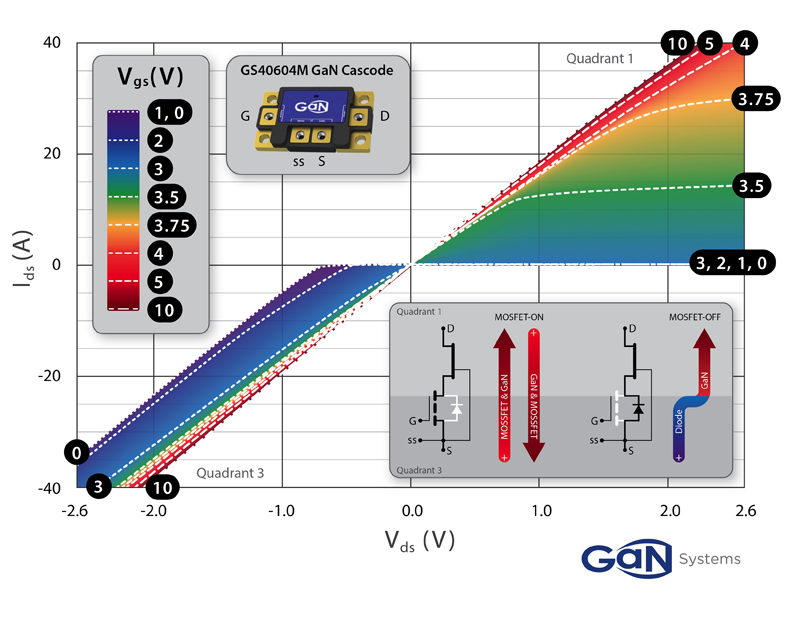
Two Quadrant Operation The normally-on GaN transistor used in the cascode is a bidirectional device. Therefore, when its gate-source voltage is held to near zero volts, the device conducts heavily regardless of whether the drain to source voltage is positive or negative. This strong conduction is shown within the red areas of Figure 2. The gate-source voltage of the GaN device can be held closely at near zero volts if the MOSFET gate voltage is kept well above 4 volts in the example shown. Below 4 volts (yellow, green, blue area) the MOSFET begins to turn off. Its on-resistance increases. The resulting voltage drop across the MOSFET debiasses the GaN device and the cascode delivers less current as shown in the yellow / green areas of Figure 2. When the MOSFET starts to turn off completely, below the blue area; cascode conduction can only occur in the third quadrant where the MOSFET intrinsic body diode provides the current path. These actions are pivotal when the device is used in certain power conversion circuits. The two quadrant mode of operation plus the significantly lower charge storage (Qrr) figure shown for the cascode allows highly efficient advanced circuitry such as the bridgeless Totem Pole PFC to be successfully implemented. The GaN cascode can have overwhelming advantages in such select applications. Gan Systems