Thermal considerations for high power chip resistors
Over the past few years, several manufacturers have developed high-power handling general purpose chip resistors covering a wide resistance range. Most of these high-power chip resistors are extensions of their general purpose commodity chip siblings, however a few offer unique heat reduction techniques that make it easier for any design engineer to use at the higher power ratings. This increased thermal energy, and how to deal with it, is the subject of much debate between electronic component users and suppliers. Today's engineers are faced with the pressure to downsize circuits or maintain the same size with additional functionality. Regardless of the application, there is a finite amount of allowable heat for each situation and the design guidelines can vary within a single market segment. Any heat above this limit must be dealt with to ensure long term reliability. Although heat generation is seldom an issue with small case size commodity chip resistors, standard 2512 and 2010 size chip resistors may experience a heat rise above 105°C. This excess heat has plagued engineers for many years. Today, the availability of higher power rated resistors is changing the methods used to handle excessive heat.
Currently, there are two basic approaches manufacturers use to achieve high power ratings on a chip resistor:
- Characterize a standard part for higher power and, in some cases, higher temperature operation
- Use improved materials, resistor design, and processes to achieve electrical performance with lower heat rise per unit power.
- Current sense and high performance, high power resistors fall under the second category. These series have proven much easier for engineers to implement into their designs.
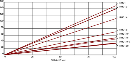
Engineers are well aware of the universal concept of tradeoffs. For example, it does the designer little good to downsize the resistors in a design if the heat generated increases such that they can't increase circuit density. If the same materials and processes are used for high power chip resistors as are used on standard commodity chips, then basic physics fundamentals would dictate that these devices would experience the same heat rise as the standard part. This begs the question, why would a design engineer specify one of these types of high power chips when there is little or no improvement in thermal performance over a standard resistor chip? The answer is that the high power rated products are characterized for use at the higher power levels and in some cases higher temperature. A standard R-Chip may show similar heat rise compared to the high power part, but what about the stability and reliability over the life of the part? What about short time overloads or pulse power handling? Maximum allowable resistance shift limits for a standard general purpose chip resistor at normal rated power are between 2% and 3%, with typical resistance shifts around 1%. The high power rating versions show similar performance at the higher power levels. Conversely, standard R-chips operating at higher power ratings have been shown to have very inconsistent performance. This may be attributed to the extreme price pressures on the commodity chip resistors forcing the use of the least expensive materials, highest process speeds, larger allowable laser trims, and the elimination of materials and processes deemed non-essential. Because high power handling resistors typically have somewhat higher average selling prices, they aren't cost constrained to the same degree.
By improving the materials and processes used in the production of high power chip resistors, the reduction in heat generated ranges from 20% to 40% depending on size. Some of the improvements used to obtain this lower heat rise include:
- Special polymer overcoats that release heat to the ambient air more efficiently.
- Unique laser trim operations designed to lower the hot spot temperatures
- Larger bottom terminations to more efficiently conduct heat into the PCB.
- However, the larger chip sizes still may generate enough heat to cause problems in the product design.
A case study done several years ago unexpectedly demonstrated the importance of power density for large size resistors. Initially the test was set up to qualify 1-watt 2512 chip resistors to AECQ200 life test. Standard test boards were designed to typical IPC guidelines and manufacturer recommended solder pads. The boards measured approximately 2-inches wide by 5-inches long and were populated with ten 2512 size standard resistor chips rated for 1 watt of power up to 70°C. This is the standard EIA and military power rating for this size and has been accepted for many years. However, the test experienced multiple failures per board before even 100 hours of testing were complete. Analysis showed charring and discoloration on all boards and was more prominent around the failed units. The test was initiated again with new parts and boards. This time the boards were monitored under a thermal scanner. The scanner showed that 1-watt of power applied to all ten units even at an ambient temperature of 25°C lead to a hot spot temperature on the board of more than 140°C. The solution was to reduce the number of parts per board from 10 to 5. The resulting hot spot temperature was just below 105°C. At the time this was the simplest and fastest solution. Most resistor users obviously don't have that luxury. For future testing, the PCB design was changed resulting in an equally dramatic improvement in hot spot temperatures.
The PCB changes tested include wider copper traces, larger land patterns, vias through the board, and the use of heavier copper for conductors. The resulting heat rise on the new boards was only 71°C. In addition to these methods, there are plenty of other heat reduction options available. Heat sinking can be used especially if there is already one being used in the design; however heat sinks are generally bulky and costly. Air movement can offer a significant improvement also, yet many designs don't have the space or end product weight flexibility to add a fan. Solder amounts and chemistry can also have a dramatic effect on thermal characteristics, but for the purposes of the above case study were held constant and ignored. Extreme power densities and power levels may require more exotic heat removal techniques, such as the use of liquid nitrogen for cooling. Some of these techniques will have a more dramatic thermal effect than others and some will substantially increase the cost as well. For example, a single layer PCB simply using heavier copper weight might make the simplest and least costly improvement. Vias through the termination and board could also be a low cost method of lowering the heat rise. However, if a customer has a 7 layer board, increasing the copper weight will typically be overkill and will increase board cost exponentially. Similarly, vias through the board would create significant routing problems for multi-layer boards. For those customers, simply placing the surrounding traces and land patterns under the solder pads would make more sense. Actual thermal improvements from these techniques can vary widely from one board to another. The specific information given here was a single case study. Much more study and testing needs to be done to provide quantifiable evidence of the improvement associated with each thermal management method. To this point, most resistor manufacturers will have some heat rise data for their highest volume products under varying conditions which should be used as a starting point for engineering design. Resistor manufacturers can control the resistor to junction thermal resistance; however the junction to PCB thermal resistance is usually a larger factor in the overall thermal profile of a given design. Ultimately, the burden falls on the design engineer to properly specify board layout, construction, and materials, as well as manufacturing parameters, such as solder material makeup and amounts per joint to maximize long term reliability at normal EIA and Mil STD power ratings and the new higher power ratings. www.seielect.com


