Increasing use of electric motors spinning at up to 100,000 rpm
The increasing use of electric motors spinning at up to 100,000 rpm, in applications ranging from electric turbochargers to surgical instruments, is creating new challenges in the design of control circuits.
The IGBT switches used in many power converters cannot switch quickly or efficiently enough to match pulse-width modulation (PWM) and control-loop-update frequencies that are rising to 100kHz. MOSFET switches can switch this fast, but are often unsuitable for high-power applications. SiC and GaN devices currently in development may offer a way forward, with both very low switching and on-resistance losses, reducing the efficiency penalty of switching at high frequencies, as well as higher power capability.
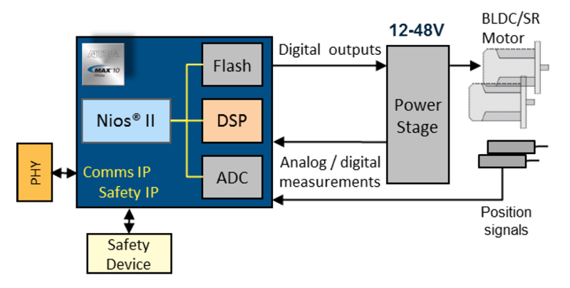
But how are we to control such high-speed systems? One approach would be to program an FPGA to create a system-on-chip including the necessary I/O and processing for multiple functions, for example both power conversion and multi-axis motor control (see Figure 1).

Click image to enlarge
Figure 1: An FPGA-based motor control system (Source: Altera)
This article describes a system architecture and scheduling mechanism for high-frequency control loops and combined motor-control and power conversion in an FPGA.
Altera’s motor control reference design
Altera provides a reference design for a ‘drive-on-a-chip’ FPGA system. It has also developed a motor-control hardware platform, the Tandem Motion-Power, for academic or commercial research, which includes:
· 12V input
· 12 - 48V DC link generated by bidirectional, 2-phase DC-DC converter
· Two 3-phase motor drives, or six half-bridge outputs
· Both analog and digital feedback measurements. Digital signals are provided by sigma-delta analog-digital converters (ADCs)
· Support for encoder/resolver/Hall motor-position feedback
· MOSFET switching transistors to support 100kHz+ PWM
· DC-DC and motor axes controlled by an FPGA development board connected via HSMC connector
The FPGA system designs described here build on these reference designs.
FPGA controller architecture options
We have tried two approaches to high-speed motor control using an FPGA. The first uses the processor to coordinate all functions. The second uses direct data connections between IP components to remove the processor from the control loops, but retains it for higher-level functions.
There are a number of design requirements to ensure maximum flexibility in the controller:
· The ability to use and compare external sigma-delta ADCs with the internal successive-approximation ADCs used in the Altera MAX 10 FPGA
· Ability to view and log data from both types of ADC using PC-based console software
· Ability to log data at the control-loop-update frequency of around 100kHz
The processor-centred approach
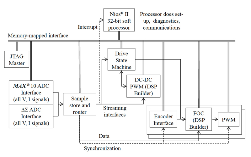
The processor-centric architecture uses a memory-mapped interface to connect all IP components. The processor is the data master. An interrupt from the drive subsystem synchronizes the processor control software to the PWM and ADC readings. The processor’s interrupt service routine (ISR) reads data from interface IP components, performs control calculations in software or via calls to accelerator IP, and writes outputs to interface IP components, including the DC-DC converter interface and drive subsystem PWM IP.
Click image to enlarge
Figure 2: A processor-centric approach to single-FPGA motor control (Source: Altera)
The processor reads both the sigma-delta and MAX 10 ADC signals. The user can select which signals to use, and view their output using the console software provided.
External IP for accelerating the DC-DC and field-oriented control (FOC) calculations was created with the Altera DSP Builder Simulink blockset.
The architecture uses multiple instances of a drive subsystem, which makes it straightforward to extend the design to multiple motor-control axes.
The standard PWM frequency is 8kHz and the control frequency is 16kHz. This architecture cannot reach very high frequencies, due to the processing time of the ISR in the processor.
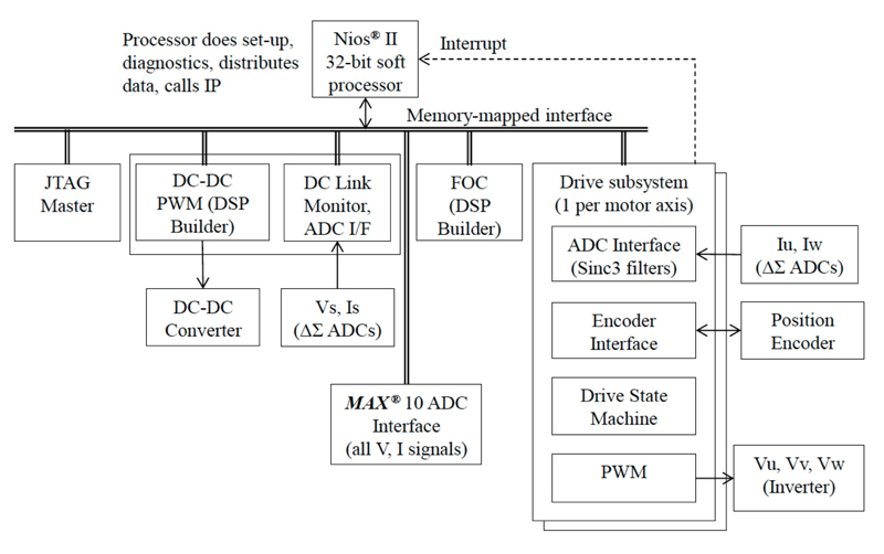
A high-frequency approach
The high-frequency architecture has a similar set of IP components, including the processor, but uses streaming interfaces to pass data from the ADC interfaces to a new sample store and router IP. This sends the data to the IP components that need it. The processor still uses an ISR to synchronize the reading of data and other operations.
Click image to enlarge
Figure 3: A high-frequency architecture takes the processor out of the control loop (Source: Altera)
There is a central ‘drive state machine’ for start-up and shutdown logic, and multiple drive subsystems, which now include the motor FOC calculations. By reducing the work done by the processor ISR and doing all motor-control operations in parallel, the control-loop update frequency can be increased to 125kHz.
Comparing the two architectures’ performance
The two architectures can be compared in terms of latency, defined here as the delay due to control-loop processing in the field-oriented current control loop and measured by the time from the centre point of the feedback measurement to the centre point of the following actuation.
Latency considerations are different for the sigma-delta ADCs and the MAX 10 ADCs.
If the sigma-delta ADCs are used, all measurements are sampled in parallel. The ADC interface uses Sinc3 filters to convert 1bit input signals sampled at 20MHz into 16bit output signals. The oversampling ratio for each Sinc filter is 128, which leads to a theoretical output sample frequency of 156,250Hz -- equivalent to a sample period of 6.4μs. The Sinc3 filter uses three such filters cascaded, leading to a total filter time of 19.2μs. The output samples are symmetrically weighted sums of the last 19.2μs of input data.
Instead of using continuous output sampling at 156,250Hz, the design takes individual readings at 16kHz, centred on the ‘quiet’ periods of the motor current waveforms at the turn-around points of the PWM counter. This reduces the filtering delay time compared to a Sinc3 filter set up for continuous output sampling at 16kHz.
Click image to enlarge
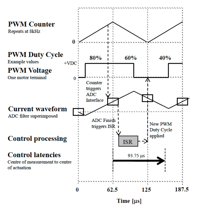
Figure 4: Control loop latency for Altera’s motor control reference design, using 8kHz PWM and 16kHz control loop updates (Source: Altera)
The timing diagram in Figure 4 shows how key signals change from the start of a measurement to a new actuation.
The PWM Counter is used to generate a PWM output of the required duty cycle, which is updated every half-PWM period. The PWM IP triggers the start of the ADC filtering 9.6μs before the centre of the reading, and finishes 9.6μs after the centre of the reading. This triggers the ISR, which completes in time to set the following PWM duty cycle. The centre point of actuation of the following PWM half-cycle is a quarter of a PWM cycle later, so the delay from measurement to actuation is 93.75μs.
Figure 5 shows the equivalent timing diagram, with timing determined by the MAX 10 ADCs continuously sampling every 8μs, repeating at 125kHz. The interfaces to the MAX 10 ADCs and sigma-delta ADCs have been adjusted to achieve a standard 125kHz.
Click image to enlarge
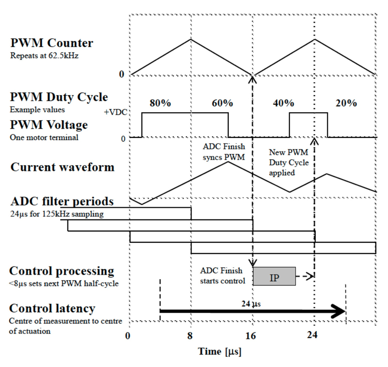
Figure 5: Control-loop latency for the high-frequency architecture using 62.5kHz PWM and 125kHz control-loop updates (Source: Altera)
When using the sigma-delta ADCs, the filtering periods for consecutive 125kHz samples are increased from 19.2μs to 24μs and overlap as shown in the diagram as ‘ADC filter periods’. If the control calculations in the FPGA’s IP can be completed in 8μs, the latency is three PWM half-cycles, or 24μs.
To summarise, the high-frequency architecture cuts latency by more than 70% from around 93.75μs to around 24μs.
A comparison of the two approaches also suggests that the resources used for the high-frequency architecture are about the same as in the processor-based design.
Conclusions
We’ve tried two architectures for a multi-axis motor control and power-conversion controller using a single FPGA.
The processor-centric architecture maximizes ease of development, as control calculations are centralized in software and fewer FPGA IP components are required.
The high-frequency design combines the benefits of a processor-based architecture, in terms of data logging, diagnostics and communication, with the low latency possible with an FPGA. This is achieved by using FPGA IP components, with both memory-mapped and streaming interfaces, to do the control-loop processing. A processor is used to collect data from the IP components and communicate high-level signals over a memory-mapped interface.
This approach, together with the Tandem Motion-Power motor-control board, provides a useful platform for developing next-generation high-frequency motor-control and power-conversion applications.