MOSFET use in low and mid power flyback topologies
Key criteria for designing power supplies units (PSU) for consumer applications are low cost, high efficiency, good thermal performance and low Electro-Magnetic Interference (EMI). Starting with an optimal power conversion topology assists the design process. Flyback topology is optimal for low and mid power PSUs. The selection of a power switch, typically a MOSFET, plays a major role in realizing the product from design to shipment. For high volume production, the benefit of a good quality MOSFET ensures low field failures.
For example, Infineon´s advanced Super Junction (SJ) principle based CoolMOS offers a significant reduction in conduction and switching losses, with a low ON resistance and gate charge, key reasons behind this performance. CoolMOS enables high power density and efficiency for advanced power conversion systems. Additionally, it covers a wide spectrum of applications from lighting and consumer to telecom and computing.
Different CoolMOS series have been developed to cover a wide range of applications. CoolMOS CE is an optimized platform for consumer applications; it offers a best-in-class price-to-performance ratio. After launching the 500 V class in 2012, the CE technology is now also available in 600 V, 650 V, 700V, and 800 V. The CoolMOS CE portfolio provides all benefits of a fast switching SJ MOSFET while retaining ease-of-use. The CE series of MOSFETs achieve very low conduction and switching losses, making applications more efficient, more compact, hence lighter and cooler.
CoolMOS CE is an optimized platform addressing and meeting consumer application needs as outlined in Table 1.
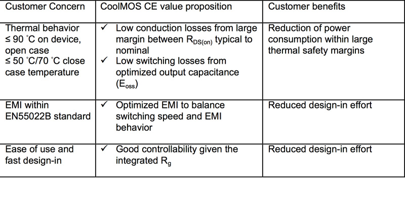
Click image to enlarge
Table 1 Consumer application needs
Improving ON-state resistance
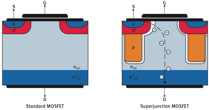
SJ technology helps to reduce the ON state resistance (RDS(on)) for high voltage MOSFETs through specialized manufacturing capabilities. In conventional MOSFETs electrons flow through a high resistance N channel, whereas in SJ technology they flow through a heavily doped n-region which lowers the value of RDS(on). The high voltage blocking is provided by adjacently placed P-columns which pass through the device close to the n+ contact (see Figure 1).
Click image to enlarge
Figure 1a & b: Cross section of standard MOSFET and Super Junction MOSFET with typical MOSFET model
Improving switching speed
CoolMOS CE is based on SJ technology where the reduction in input and output capacitance results in lower switching and driving losses. Because of this capacitance reduction the Eon and Eoff of the CE device is half that of a standard MOSFET. Furthermore, the reduction of capacitance results in a reduced gate charge (Qg), which gives the benefit of reduced driving losses and the ability to use lower drive currents.
Capacitance role in switching performance
A fundamental characteristic of SJ devices is that both the output and reverse capacitance show strong non-linearity. The non-linearity in SJ capacitance characteristics comes from the fact that at a given voltage – typically in the range of 1/10th of the rated blocking voltage – p- and n-columns deplete each other leading to a fast expansion of the space charge layer throughout the structure.
This means that at a voltage beyond 50 V, for 500 V rated devices both output and reverse capacitance reach minimum values of only a few pF. This is resulting in a dv/dt of more than 100 V/ns and di/dt of several thousand A/μs if the load current is allowed to fully commute into the output capacitance during turn-off.
The voltage rise is therefore proportional to the load current and inversely proportional to the value of the output capacitance (Coss). As Coss decreases as voltage rises, the highest dv/dt is reached shortly before reaching the bus voltage. The corresponding di/dt is mainly limited by the inductance of the package and printed circuit board (PCB). The highest efficiency can now be reached by turning-off the device in this manner, because the switching losses can be reduced down to the level of the stored energy in the output capacitance. All these benefits will be clearly visible in the efficiency performance.
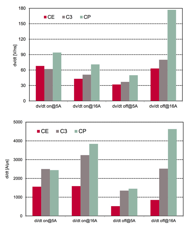
CE devices have a smooth characteristic and show dv/dt of less than 70 V/ns and di/dt of less than 900 A/us as shown in the pictures below. CE has a built in ease-of-use making it optimal for designers facing a short time to market (see Figure 2)
Click image to enlarge
Figure 2: Comparison of CE switching characteristics
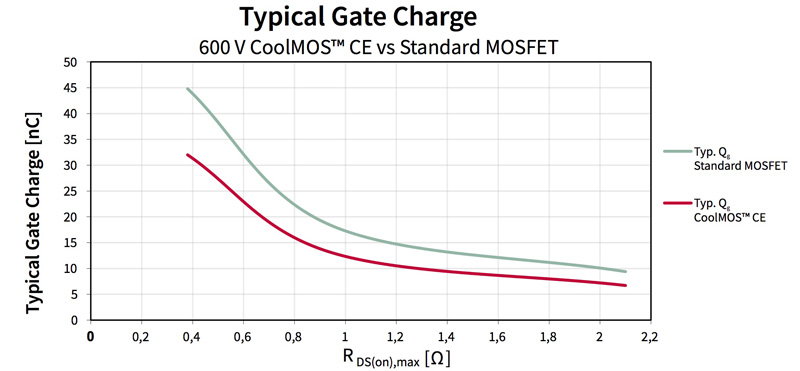
Key parameters: Gate charge (Qg)
One of the most important improvements is Qg reduction which brings benefits, especially in light load conditions, due to reduced driving losses. CoolMOS CE has approximately 40 percent Qg reduction in comparison to a similar standard MOSFET over the entire RDS(on) range. Figure 3 shows the Qg in nanocoulombs (nC) of the 600 V CE against a standard MOSFET over the RDS(on) max range from 400 mΩ to 2100 mΩ.
Click image to enlarge
Figure 3: Qg comparison 600 V CE vs. standard MOSFET
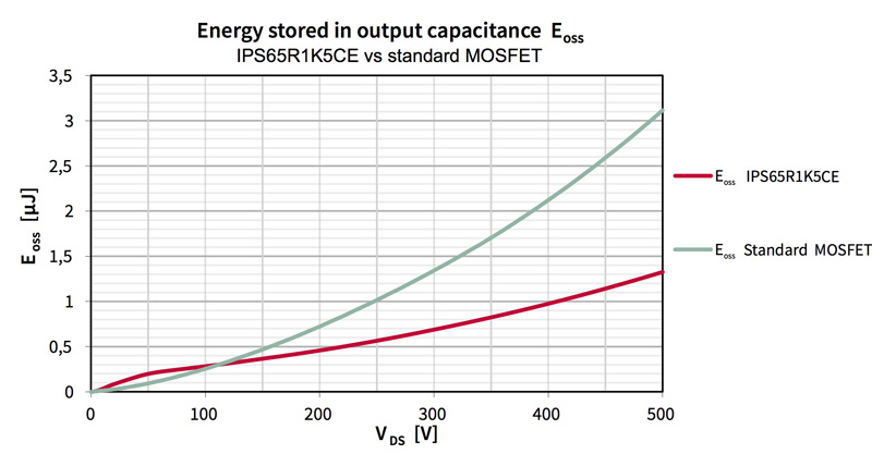
Energy stored in output capacitance (Eoss)
The reduced energy stored in the output capacitance brings an important difference in hard switching topologies and also reduces switching losses in a resonant topology. Normally it is possible to choose between zero voltage switching (ZVS) or zero current switching (ZCS). In these two cases it is possible to eliminate the turn-on losses (ZVS) or the turn-off losses (ZCS), but it is not possible to work in these two operation modes at the same time.
Typically for MOSFETs the ZVS operation is preferred due to the usual important contribution of the output capacitance to the turn-on losses (if hard switching). Therefore, one part of the switching losses is still always present, and the reduction of Eoss brings a reduction of those switching losses. Figure 4 represents the Eoss comparison between the 650 V CE and a comparable standard MOSFET of 1500 mΩ devices.
Click image to enlarge
Figure 4: Eoss comparison 650 V CE vs. standard MOSFET
The Eoss loss is in direct proportion to the output capacitance as a function of drain to source voltage (VDS) of the MOSFET. In this case the effect of a reduction of Coss is very visible. One further benefit is a faster VDS transition time in resonant topologies, which means that it is possible to reduce the resonant inductance and circulating current loss, because it is possible to completely discharge the Coss with lower currents.
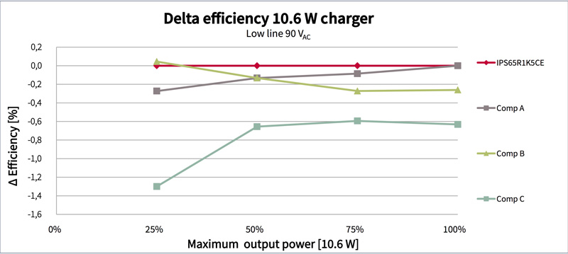
In order to show the performance results of CoolMOS CE in a flyback application a comparison is made between CoolMOS CE and other MOSFETs.
In this measurement the 650 V CE is compared to a standard MOSFET in the 1.5 Ω RDS(on) range for a 10.6W adapter (see Figure 5).
Click image to enlarge
Figure 5: 650 V CE vs. standard MOSFET efficiency difference comparison @ Vin = 90 VAC
Topology: Peak current controlled flyback
Vin = 90 VAC – 264 VAC
Vout = 5.3 VDC
Iout = 0 A to 2 A
Switching Frequency = 50 kHz @ full load
Ambient temperature = 25°C
Plug and play scenario between 650 V CoolMOS CE and standard MOSFET
High voltage MOSFET = IPS65R1K5CE
This plug and play measurement shows the benefit of a SJ MOSFET in comparison to a standard MOSFET in terms of efficiency and thermal performance. Due to the Qg reduction of CoolMOS CE technology, better average efficiency can be obtained. Thus high efficiency requirements can be easily achieved with this CoolMOS CE
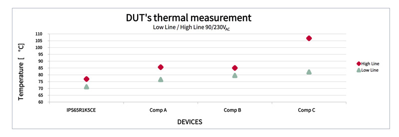
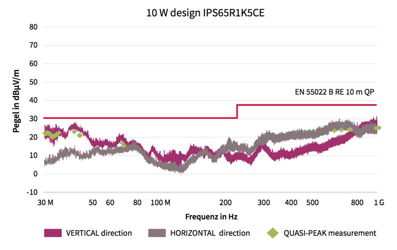
The thermal behavior of the power devices in an adapter application is very critical because it is difficult to dissipate the heat generated by components due to very dense construction and high thermal resistance of the casing. Therefore, power MOSFETs with improved switching losses will help in ensuring the device is below the temperature limit. As presented in Figure 6, IPS65R1K5CE offers 5°C lower than the nearest competitive device at low line (worst case). Furthermore, the design meets EMI specifications with sufficient margin as shown in Figure 7.
Click image to enlarge
Figure 6: 650 V CE vs. standard MOSFET thermal comparison
CoolMOS CE has proven to be a cost competitive MOSFET technology which is used to provide the good efficiency needed for meeting environmental energy standards. Its lowest on resistance and low gate charge help maintain the low thermal profiles needed for safety compliance. The integrated gate resistor for optimized switching performance helps mitigate EMI problems arising due to less than optimal PCB layout. CE devices come with a wide range of package options which enable sleek designs and have many ON resistance choices to facilitate modular designs. With Infineon´s production capacity and quality record, the CoolMOS CE is ideally suited for consumer applications.