EV’s benefit from CoolSiCTM MOSFET
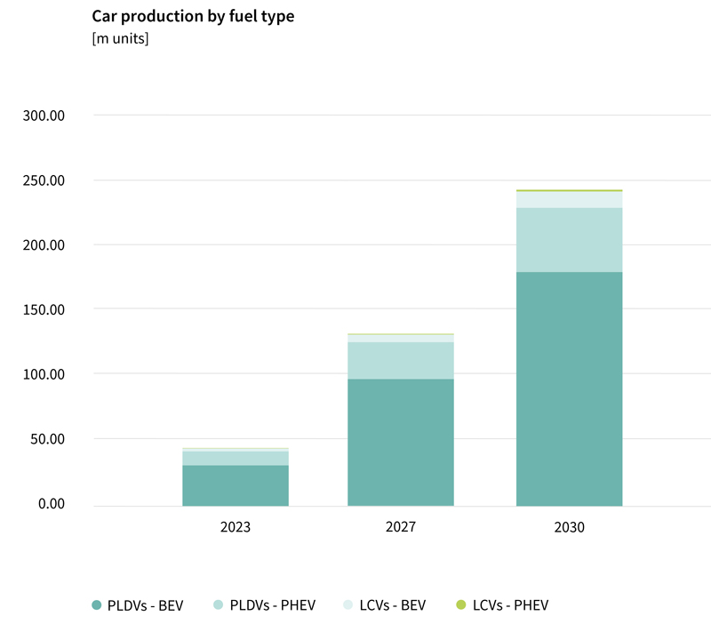
Figure 1: Electric vehicle stock by mode in the Announced Pledges Scenario, 2022-2030 IEA Global EV Outlook 2023
CoolSiC™ MOSFET 750 V G1 from Infineon Make Onboard Chargers Smaller, Lighter and More Efficient
The International Energy Agency (IEA) predicts that by 2030, 60 percent of the automobile market will consist of electric vehicles (EV), resulting in over 200 million electric powertrains on the road (Figure 1). In addition to this rapid growth, the automotive industry must integrate various other trends, such as automation, connectivity, and security, creating a dynamic environment for power electronics designers to work in. This poses a challenge particularly for designers of onboard chargers (OBC) for electric vehicles, who must constantly respond to increasing efficiency targets, reduced available space, and innovative integration concepts. Engineers are pursuing highly ambitious design targets to stay ahead of the game. To that end, Infineon's automotive-qualified CoolSiC™ power MOSFET 750 V G1 provides OBC designers a better alternative to traditional silicon (Si) devices, giving them an edge in the automotive industry.
Infineon's automotive CoolSiC™ MOSFET 750 V G1 responds to current EVs trends
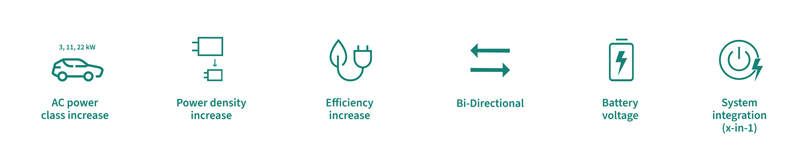
Infineon has identified six key trends (Figure 2) related to OBCs and other high-voltage applications that can be directly addressed with silicon carbide (SiC) MOSFETs:
- Increased charging power: Power levels in OBCs for EVs are gradually increasing from 3.6 kW to 7.2 kW, 11 kW, and even 22 kW while also adopting three-phase system designs, increasing the overall number of switches required per system.
- Need for higher power density: Higher switching frequencies help reduce the overall converter size by shrinking the transformers and other passive components. SiC devices run more efficiently at higher switching frequencies than Si devices, enabling system designs with power densities increasing from 2 to 4 kW/l.
- Maximizing efficiency levels: With increasing charging power and limited available space, new converter designs need to run more efficiently to avoid overheating. SiC MOSFETs play a critical role here by significantly reducing losses compared to Si alternatives.
- Bidirectionality: With increasing use cases for bidirectional power flow such as vehicle-to-grid (V2G) or vehicle-to-load (V2L), the functionalities of OBCs are being extended. SiC is a key enabler for bidirectional topologies because of the motor operation of the topologies used, and system designs need to be updated to such a new feature offered by the car manufacturers.
- 400 V and 800 V batteries: Battery voltage levels in the luxury vehicle segment are increasing to 800 V, presenting a mixed picture of 400 V and 800 V batteries that demand different charging solutions. Infineon offers a diversified SiC portfolio in 750 V and 1200 V, which can be used in various topologies to address a wide range of requirements.
- System integration (x-in-1):The evolution in EV design will demand highly integrated systems (i.e., motor + gear box + inverter + onboard charger + DC/DC converter + battery management system + power distribution unit + thermal management + PTC (Heating)) to improve cost-effectiveness. Infineon's top-side cooling portfolio of efficient power switches perfectly enables this trend.
Click image to enlarge
Figure 2: Main trends related to high-voltage applications in EVs
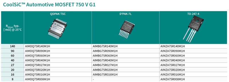
Infineon's first generation of automotive-qualified CoolSiC™ MOSFET 750 V G1 helps OBC designers stay ahead of these trends. These MOSFETs come in a variety of packages, including TO-247-4, D2PAK-7, and the QDPAK TSC (top-side cooled), and in a very granular portfolio with typical RDS(on) values starting as low as 8 mΩ, all the way up to 140 mΩat 25°C (Figure 3).
Click image to enlarge
Figure 3: Infineon’s CoolSiC™ MOSFET 750 V G1 portfolio
These devices offer OBC designers several advantages over Si devices (Figure 4), including:
- Lower RDS(on) temperature coefficient: CoolSiC™ MOSFET 750 V G1 has a lower RDS(on) with a temperature coefficient up to 27 percent lower than Infineon's 650 V CoolMOS™ CF7DA devices, the latter having set the benchmark for Si MOSFET performance. This results in lower conduction losses for SiC devices compared to Si devices at the same operating temperature.
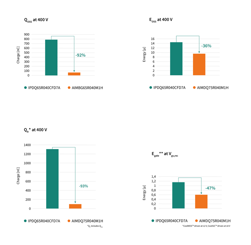
- Drastically reduced Qoss and Qfr enable hard-switched half-bridge topologies: Again, using the 650 V CoolMOS™ CF7DA as a benchmark, the Qoss value for the CoolSiC™ MOSFET 750 V G1 is almost an order of magnitude lower (92 percent). This has significant advantages for applications employing zero voltage switching (ZVS) as it reduces the magnitude of current required and the transition time for a given current level. In addition, a 93 percent lower Qfr in SiC reduces switching cycle losses and enables cycle-by-cycle hard commutation of the body diode in, for example, continuous-conduction mode (CCM) totem-pole power factor correction (PFC) or other similar topologies.
- Reduced hard switching losses in single-ended topologies: 36 percent lower Eoss in the CoolSiC™ MOSFET 750 V G1 also makes it an effective replacement for 650 V CoolMOS™ CFD7A in single-ended topologies like the classic boost converter.
- Increased light-load efficiency in high-frequency resonant topologies: Egate in CoolSiC™ MOSFET 750 V G1 is 47 percent lower than that in 650 V CoolMOS™ CF7DA devices, a feature which, together with the low Qoss, improves light-load efficiency.
Click image to enlarge
Figure 4: CoolSiC™ MOSFETs deliver significant performance improvements over silicon
750 V CoolSiC™ MOSFETs simplify system design while delivering highest quality and robustness for automotive applications
While delivering significant benefits for various power topologies, Infineon's CoolSiC™ MOSFET 750 V G1 brings additional system-level benefits that help simplify designs. These MOSFETs boast the lowest parasitic capacitance within their class, reducing switching losses and associated heat dissipation, thus simplifying system cooling requirements. The devices are robust against parasitic turn-on (PTO), which enables unipolar driving, eliminating the need for negative off-state voltage and simplifying gate-driving circuitry design. Even so, they remain compatible with 15 V on-state voltages for seamless dual-sourcing.
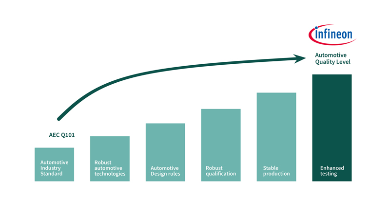
All Infineon CoolSiC™ devices are constructed using the proven gate-oxide layer and trench gate technology features, offering a unique SiC quality. Additionally, CoolSiC™ MOSFET 750 V G1 offers best-in-class robustness and cosmic radiation ruggedness thanks to a higher breakdown voltage. This technology fulfills and exceeds AEC Q101 automotive standards in numerous ways (Figure 5). This unique combination of features brings the added reassurance of superior device robustness and long-term dependable performance in safety-critical automotive applications.
Click image to enlarge
Figure 5: Infineon's device features are optimized for automotive-quality requirements
Enabling higher power density and reduced manufacturing effort with Infineon's top-side cooled CoolSiCTM G1 MOSFETs
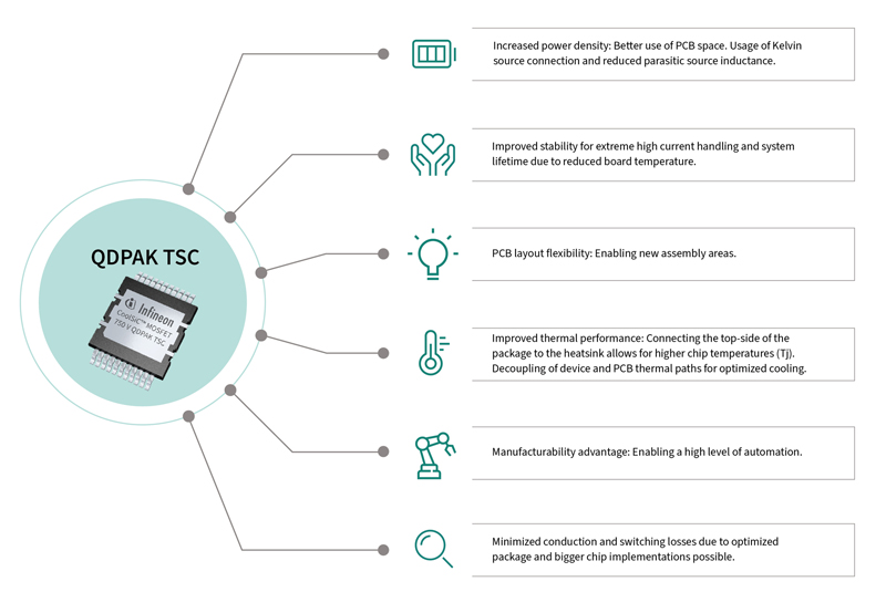
A key component to achieving challenging power density levels beyond 4 kW/I for OBCs is the device package, as it determines the cooling infrastructure. For instance, when through-hole-packaged devices are used, the cooling channels must have a specific structure and dimensions to keep the devices within a safe operating temperature range, which leads to larger cooling form factors. Infineon's innovative, top-side cooled QDPAK package, housing the 750 V CoolSiC™ G1 MOSFETs, enables increased power density by better use of PCB space. The Kelvin-source connection and lower parasitic source inductance reduce switching losses at high currents, extending the system lifetime by shrinking the device and board temperature. PCB layout is more flexible, allowing for new assembly areas. By directly attaching the packages to the exposed OBC enclosure using a thermal interface, heat dissipation is faster. Connecting the top side of the package to the heatsink improves the thermal performance, allowing higher power dissipation and lower chip temperatures (Tj). This advantage enables a high level of automation by reducing the manufacturing effort for OBCs and keeping costs down. The decoupling of the device and PCB thermal paths for optimized cooling minimizes conduction and switching losses, thus improving efficiency. Ultimately, Infineon's top-side cooled CoolSiC™ G1 MOSFETs enable OBCs to deliver more power from smaller enclosures, reducing charging times for vehicle owners and making electric vehicles a more attractive proposition for consumers (Figure 6).
Click image to enlarge
Figure 6: Top-side cooling offers a multi-level value proposition for OBC designs
Infineon's wider semiconductor technology portfolio supports various OBC designs
While CoolSiC™ MOSFET 750 V G1 solves many of the power density issues, Infineon also offers a broad portfolio of Si superjunction (SJ) and gallium nitride (GaN) devices, which can benefit these designs in various ways. This portfolio includes devices with a broad range of RDS(on) values, voltage classes, and package options, allowing Infineon to help designers create the most suitable solutions according to their needs. For example, Infineon recommends design-optimization using a hybrid solution in the totem-pole PFC stage – combining CoolSiC™ MOSFETs in the high-frequency leg with Si SJ CoolMOS™ (or CoolSiC™ Hybrid) switches in the low-frequency leg. This hybrid arrangement is also usable in high-voltage DC-DC converters based on switching frequency and efficiency demands.
Since every power transistor requires a driving circuitry, Infineon offers specific gate drivers such as EiceDRIVER™ 2EDR8258XQ1, 2EDR8259XQ, and 2EDR8259HQ1with the appropriate driving voltages, delay times, common-mode transient immunity (CMTI), and isolation requirements (non-isolated, functional, or reinforced) to optimally drive the various Infineon power MOSFETs. Infineon also offers reinforced isolated digital isolators such as ISOFACE™ digital isolator 4DIR1400HA, 4DIR1401HA, 4DIR2400HA, and 4DIR2401HA, which can greatly simplify PCB layout creepage and clearance requirements when combined with an appropriate gate driver.
Conclusion
To remain competitive in the ever-changing electromobility market, OBC design engineers will continue to strive to meet increasingly ambitious efficiency and power density targets.
The AEC Q101-qualified CoolSiC™ MOSFET 750 V G1 family is the latest addition to Infineon's continuously expanding portfolio of Si, Si-SJ, and wide-bandgap devices, which can assist designers of OBC and HV-LV DC-DC converters in outperforming their competition and reimagining converter designs.
Click here- for more information on Infineon's CoolSiC™ MOSFET offering.
To browse our solutions for OBC designs, visit the dedicated website – click here.