Technology behind the SiC MOSFET and applications
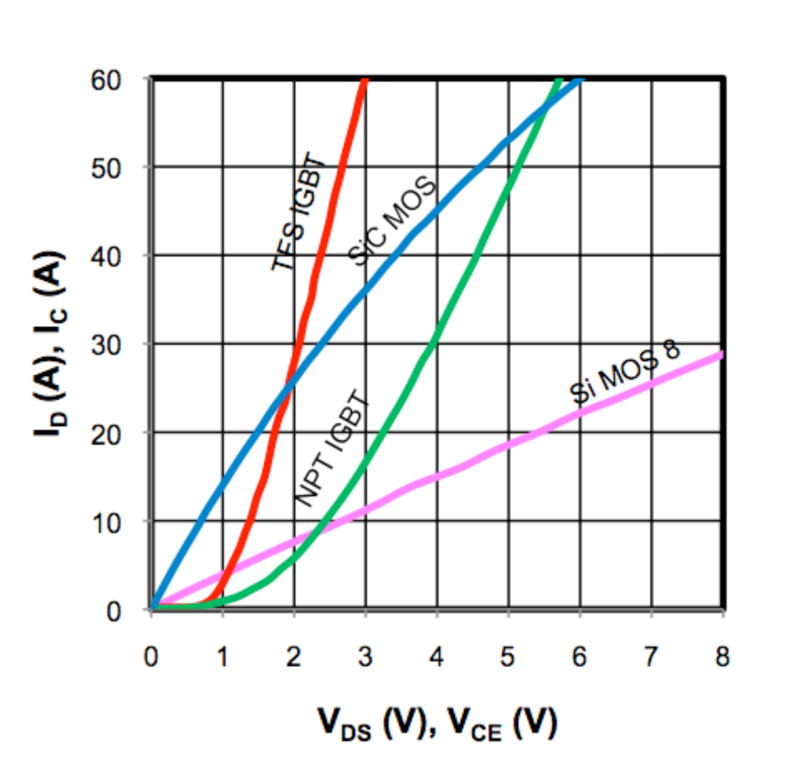
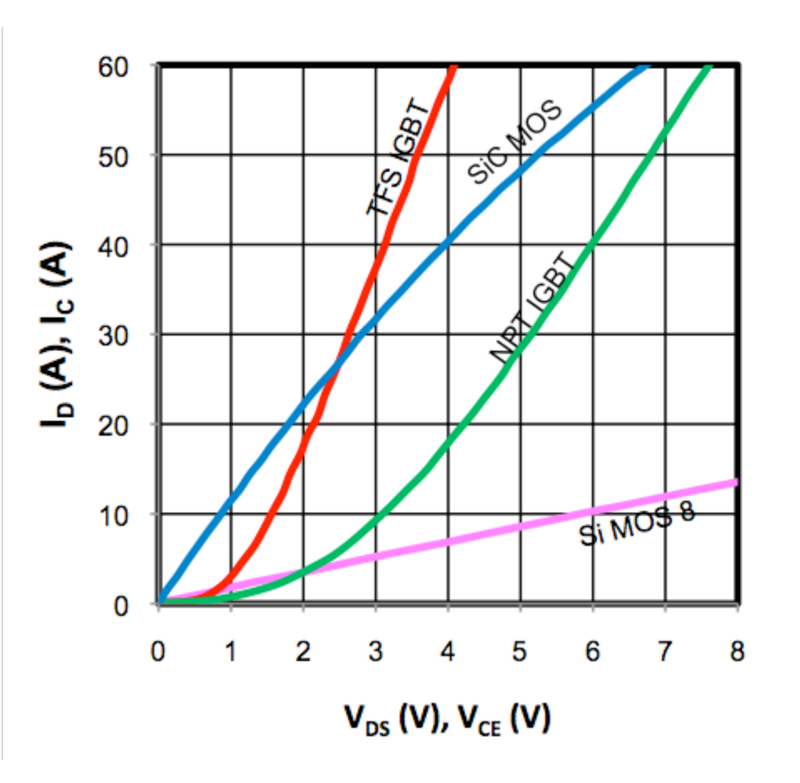
Figures 1 &2: Forward conduction characteristics comparison
Silicon carbide (SiC) is a compound semiconductor that is superior to silicon (Si) in several respects. These advantages stem from SiC's ~10x higher critical breakdown field, ~2.8x higher thermal conductivity, and ~3x higher bandgap compared to Si. For the future, the compelling cost of ownership over lifetime argument could find these devices in future everyday appliance applications. The higher critical breakdown field allows for a much thinner device for a given breakdown voltage. This reduces the on-resistance per unit area by as much as two orders of magnitude compared to Si. Conversely, the higher breakdown field of SiC also allows the realization of SiC MOSFETs with voltage ratings up to 10kV. The higher thermal conductivity allows higher current density capability for a given junction temperature. Lastly, the wider bandgap of SiC over Si affords about 1 to 2 orders of magnitude lower leakage current at high temperatures. The advantages of the 1.2kV SiC MOSFET technology are best illustrated by a comparison with existing 1.2kV Si switches. The forward conduction characteristics of the SiC MOSFET, along with a Si MOSFET, TFS, and NPT IGBTs are presented in Figures 1 & 2.
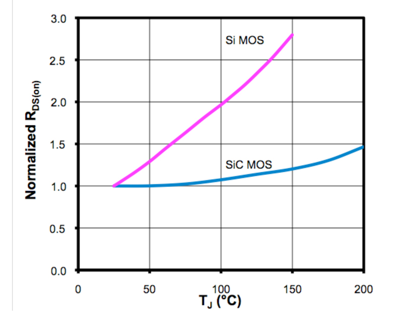
At 150°C, the RDS(on) of the SiC MOSFET increases only about 20% from 25°C to 150°C whereas the Si MOSFET device's RDS(on) increases by 250%, as shown in Figure 3. This has a significant effect on system thermal design.
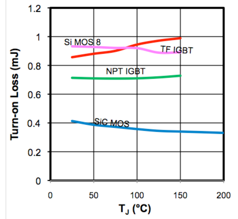
Being a majority carrier device, the SiC MOSFET does not have a minority carrier current tail like the Si IGBT. This results in significantly lower switching losses and allows easy paralleling. The inductive switching loss versus temperature is shown in Figure 4. In all cases, the SiC MOSFET switching losses are significantly better than its silicon competitors.
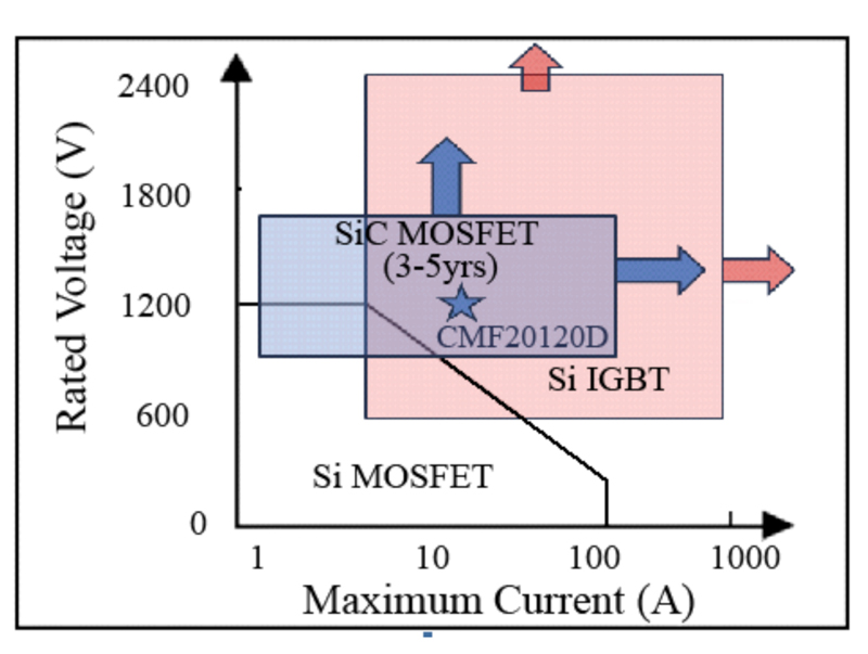
In general, the 1.2kV SiC MOSFET can be used in almost any application presently using a 1.2kV Si MOSFET or 1.2kV Si IGBT, where higher efficiency and higher operating frequency are desired. These applications can vary from solar and wind inverters and motor drives to induction heating systems and high voltage DC/DC converters. The application space for the SiC MOSFET is shown in Figure 5.
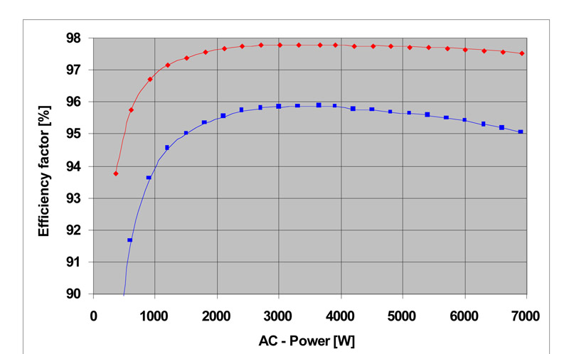
The solar inverter application will illustrate the value proposition of SiC MOSFETs. The comparison vehicle was a 7kW, 16.6kHz three-phase grid connected solar inverter employing a B6 topology developed by the Fraunhofer Institute. This topology uses a split link DC capacitor with a connection of the neutral conductor to the center point of both capacitors. The unit connects to a 400V grid, therefore 1.2kV IGBTs are used for the switching devices. The Si IGBTs were directly replaced with 1.2kV SiC MOSFETs, with no circuit optimization and this resulted in a significant improvement in efficiency as shown in Figure 6. The SiC MOSFET improved the maximum efficiency by 1.92%, and the overall European efficiency rating improved by 2.36%. This equates to a 50% reduction in overall losses in the system. Furthermore, the heat sink temperature was reduced by 43 °C. Further research has also been conducted with these devices by ISET (Institut fur Solare Energieversorgungstechnik) & SMA GmbH, yielding a 99% maximum efficiency rating in their three-phase grid connected system. Another application for SiC MOSFETs is motor drives. An experiment was performed at Cree [6] where the Si IGBTs were directly replaced with SiC MOSFETs in a 230VAC 2.2kW three-phase motor drive operating at 16kHz. The SiC MOSFETs demonstrated a 2% efficiency improvement along with a 50% reduction in heat sink temperature. In both the solar inverter and motor drive, the losses are essentially cut in half. This allows substantial simplification of the cooling systems, such as elimination of fans, etc. Furthermore, higher operating frequencies (48kHz+) are possible, allowing for significant reductions in the size and weight of inductors and EMI filters. SiC MOSFETs find application in three-phase 480V power factor correction circuits where 1.2kV switching devices are required. The Si MOSFET has excessive conduction loss at this voltage, whereas the Si IGBT has higher switching loss, thus limiting the practical upper operating frequency. The combination of low conduction and switching losses makes the SiC MOSFET ideal for this application, promising higher efficiency and the ability to operate at higher frequencies, thus reducing the size of the inductive components. High power converters are employed for welders, plasma cutters, and other industrial equipment. The same issues occur for these applications when a 1.2kV switch is required. To efficiently operate Si IGBTs at frequencies above approximately 24kHz, resonant topologies need to be employed involving the use of additional resonant components and usually result in higher transformer RMS currents per unit of output power. An alternative to this is to use a multi-level topology using lower voltage Si MOSFETs, which requires doubling the number of switches. The high frequency capability of SiC MOSFETs allows the use of simple two-level hard switched topologies. A 10kW, 1kV DC-DC converter operating at 32kHz (hard switched) has been demonstrated with over 97% efficiency. Summary: SiC technology represents a fundamental change in power electronics. The price of a SiC MOSFET is more expensive than a Si MOSFET or Si IGBT. However, the entire system and energy savings potential need to be considered in assessing the overall value proposition that this technology delivers. The following system savings need to be carefully considered: Reduction of the cost of passive components In many instances, the cost of the passive power components dominate the overall bill of materials cost. Increasing the switching frequency provides a means to reduce the size and cost of these devices. Reduction in cooling requirements The significant reduction in heat sink temperatures by up to 50% has been observed with this technology allowing a reduction in heat sink size and/or the elimination of fans. Reduction in energy costs over the life of the equipment The usual temptation is to consider only the component and manufacturing cost of a system in calculating the value proposition. It is very important to consider energy savings when considering the value proposition of this technology. The energy cost savings over the life of the equipment is a significant, if not the dominant part, of the value proposition of this technology. This especially applies to solar inverter applications, where cost savings are dependent on inverter efficiency. A 40% to 50% reduction in power losses is a strong economic advantage. www.cree.com