Creating Material to Miniaturize Telecommunication Devices
WASHINGTON, D.C. -- Modern communication systems often employ optical fibers to carry signals across or between devices. The integrated optics in these devices combine more than one function into a single circuit. However, signal transmission requires long optical fibers, which makes it difficult to miniaturize the device. Instead of long optical fibers, scientists have started testing planar waveguides.
In the Journal of Applied Physics, from AIP Publishing, investigators from the University of Leeds report on a laser-assisted study of a type of glass that shows promise as a material for broadband planar waveguide amplifiers. This material is made by doping a type of glass made from zinc, sodium and tellurium with the rare earth element erbium. Erbium-doped waveguide amplifiers have garnered attention because electronic transition for erbium occurs at the same wavelength, 1.5 microns, that is a standard in telecommunications technologies.
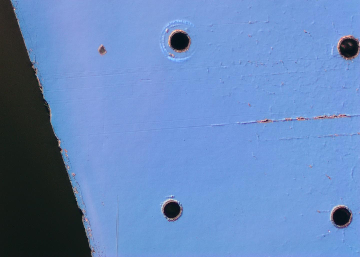
While a planar waveguide guides light along a single geometric plane, the investigators used a technique known as ultrafast laser plasma doping that utilizes ultrafast lasers to incorporate erbium ions as thin films in a silica substrate. The researchers aimed a high-intensity laser at the surface of the erbium-doped glass, which blasted a tiny crater and produced a thin film from the plume of ejected material.
Their measurements during the film formation process focused on the ablation threshold of the glass. This quantity describes the minimum energy required to separate atoms or molecules by intense laser irradiation. The investigators determined how the ablation threshold in their system was affected by the radius of the laser beam, the number of laser pulses and the concentration of the erbium ion dopant.
They found that the ablation threshold does not depend on the low doping concentration of erbium ions needed to engineer any device. Although this study focused exclusively on erbium ions as the dopant, "This result could be applicable to other dielectric materials processed with ultrafast lasers," said Thomas Mann, an author on the paper.
The investigators also looked at the shape and characteristics of the tiny craters blasted into the glass. Understanding the morphology of craters produced during the fabrication process is important for controlling properties such as the porosity, the surface area, and the ability of the material to scatter or absorb light.
"These properties are important for engineering other dielectric materials for surface area-demanding applications in photocatalysis, sensing, fuel and solar cells, and light extraction in LEDs," Mann said. The next phase in their research will involve more precise engineering of thin films and waveguides for amplifiers, sensors and other devices.
EurekAlert!, the online, global news service operated by AAAS, the science society: https://www.eurekalert.org/pub_releases/2018-07/aiop-btc072018.php


.jpg)
