DC-DC Conversion for 48 V – 12 V Automotive Applications
Dual 48 V and 12 V Bus for Mild Hybrid Vehicles
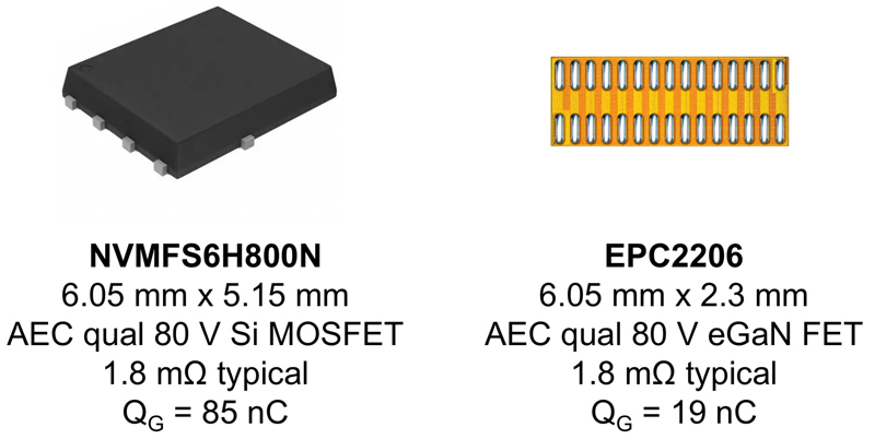
Figure 1: Example comparison of AEC qualified Si MOSFET and eGaN FET
Recent evolution in automotive powertrain technology has motivated the use of a dual 48 V and 12 V bus in mild hybrid vehicles, which can provide an 8 − 15% fuel consumption reduction. The 48 V Li-ion battery bus furthermore supports higher power loads such as air conditioning, faster heating of the cabin, and faster, smoother starting. To support legacy 12 V systems, there is a need for a bi-directional 48 V – 12 V DC-DC converter system.
GaN transistors, with favorable figures of merit (FOM) for 48 V applications, can provide a reduction in size, weight, and bill of material costs. This article presents a five-phase, fully regulated, bidirectional 48 V to 12 V DC-DC converter. An advancedthermalmanagement solution suitable for use with eGaN FETs results in a system that can provide 3kW of power at an efficiency exceeding 97.5% into a 14.5 V battery.
GaN Advantages in 48 V Systems
The performance of a bi-directional 48 V and 12 V non-isolated multi-phase synchronous buck converter can be enhanced with high-performance wide bandgap gallium nitride transistors. eGaN FETs offer up to a four-fold size and switching figure of merit reduction over state-of-the-art silicon MOSFETs at 80 - 100 V. Additionally, with automotive qualification (AECQ-101RevD),theycanprovideareliable, efficient, and higher power density alternative to Si MOSFETs for automotive power delivery applications.
An example of the size difference between AEC-qualified Si MOSFETs and GaN FETs is shown in Figure 1. Both are 80 V devices and have comparable RDS(on), although the total gate charge, QG, is considerably higher for the Si MOSFET than the EPC2206 eGaN FET. This means that the GaN FET is expected to outperform the Si MOSFET from light load through to high current. Additionally, the eGaN FET has the thermal advantage of six-sided cooling, so it can handle much higher current than its siliconcounterpart.
eGaN FET-Based, Five-Phase High Current Bi-Directional DC-DC Converter
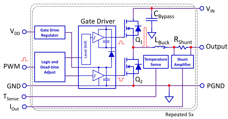
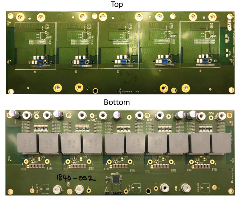
The power circuit schematic and photo, top and bottom view, of the five-phase proof of concept high current bi-directional 48 V and 12 V DC-DC converter are shown in Figure 2. The PCB is 4 inches (100 mm) by 11 inches (280 mm) and consists of six layers, with 1.6 oz. copper on the outer layers and 2 oz. copper on the four inner layers.
Each phase uses two automotive-qualified 6.8 µH inductors, Vishay IHLP-8787-GZ- ER6R8M5A, connected in parallel to support the required saturation current. This prototype uses the LMG1205 gate driver from Texas Instruments, an LT6105 current sense amplifier and the AD590 temperature sensor, both from Analog Devices. The eGaN FET used is the AEC Q-101 qualified EPC2206. The prototype is regulated in a closed loop to 12 V or 14.6 V, depending on the requirement.
Click image to enlarge
Figure 2a: Power circuit schematic
Click image to enlarge
Figure 2b: Photo of the five-phase prototype using EPC2206 GaN FETs
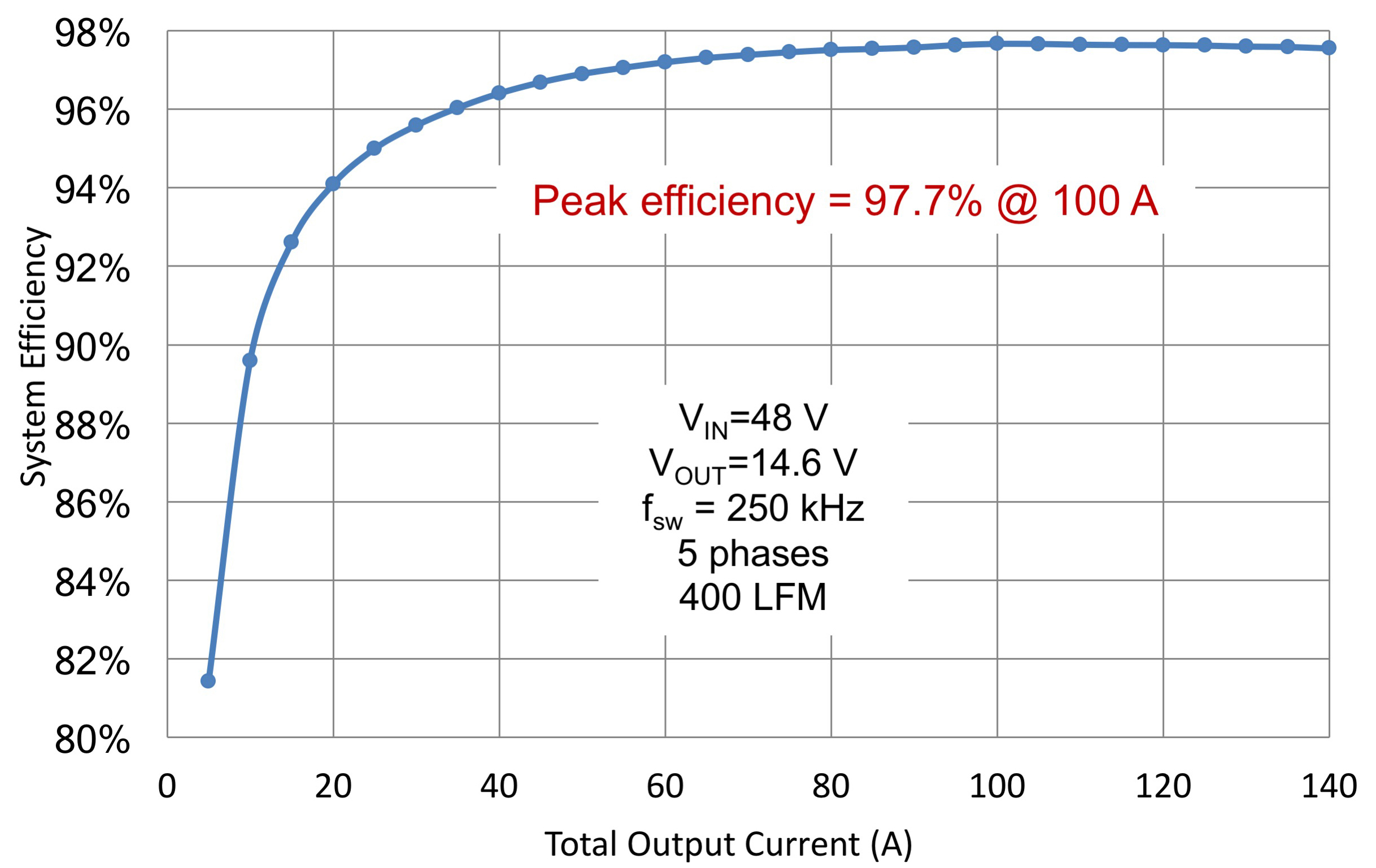
Initially, the performance of this multiphase converter was evaluated with no heatsink, and with approximately 400LFMforcedairappliedtothePCBforthermal management and operated at 250 kHz. For automotive applications, the switching frequency, fsw, cannot be too close to 500 kHz because of possible AM band interference. In traditional Si-based systems such as, switching frequencies closer to 100 kHz are chosen due to the high QG of Si MOSFETs.
However, eGaN FETs offer the promise of moving to higher switching frequencies to reduce the size and increase overall system efficiency. This is seen in Figure 3, where a peak system efficiency of 97.7% was achieved.
Click image to enlarge
Figure 3: Efficiency at fsw = 250 kHz and 140 A is 97.7% with no heatsink present.
High-Performance Thermal Solution
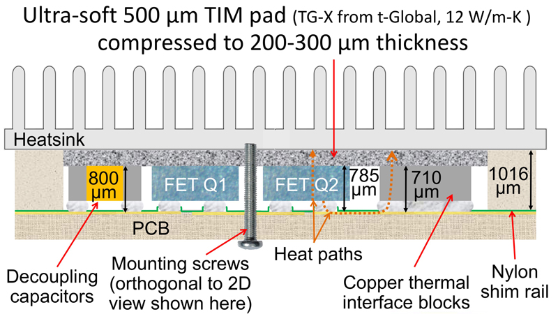
Chip-scale eGaN FETs offer up to six-sided cooling, enabling effective heat extraction from the bottom, top, and sides of the die. Figure 4 shows the cross-section of a suitable thermal approach for eGaN FETs where all components are on the same side of the board as the FETs, which will be cooled by the heatsink, are either the same height or lower. Copper thermal interface blocks are used to reduce the thermal resistance between the copper and heatsink.
Click image to enlarge
Figure 4: Cross section of the enhanced six side thermal solution for the eGaN FETs.
To maximize the benefit of double-sided cooling, a connection of a heatsink to the top side of the PCB using a nylon shim to mechanically set the gap between the FETs and heatsink. Additionally, a gap-pad thermal interface material (TIM) was compressed within this gap to reduce the thermal resistance between the heatsink and FETs, while also extracting heat from the PCB in the surrounding area. This method is explained in Efficient Power Conversion’s How2AppNote 012.
In this design, shown in Figure 5, copper thermal interface blocks (TIBs) are also soldered to the copper planes connected to both FETs. Use of TIBs further improves the heatsink’s ability to extract heat from the FETs through Rθ, jb, in parallel with the primary path through Rθ,jc. The TIBs and other nearby components are selected to be lower profile than the FETs (0.031 inches / 0.785 mm), and the height of the plastic shim is set at 0.04 inches (1 mm) to maintain a very low thermal resistance between the FET and the heatsink and apply the correct compression force for the thermal interface material.

Click image to enlarge
Figure 5: Board to heatsink assembly showing the nylon shims installed the and 0.5 mm TGX thermal pads placed over power stages.
Heatsink Results
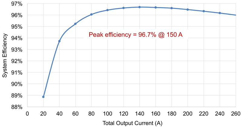
The prototype was tested with 400 LFM forced air and natural convection cooling. The forced air condition was tested first, with a maximum output power of 3.12 kW. Five phases were operated at 120 kHz and 12 V output, with up to 52 A per phase. The peak efficiency was measured at 96.7% at an output current of 150 A, and the maximum junction temperature was estimated to be 53°C based upon the on-board temperature measurements using the calibration data for those sensors. The measured phase currents were well-balanced to within 3% between each phase.
Click image to enlarge
Figure 6: Efficiency at 48 V – 12 V conversion 400 LFM forced air cooling across the heatsink.
The system was then tested with natural convection cooling. This test concluded at 200 A total output current (2.4 kW) to maintain the junction temperature below 100°C.
Conclusions
Focused on improving efficiency, reliability, and power density for 48 V to 12−14.5 V power conversion for automotive applications, a five-phase bi-directional 3 kW buck/boost prototype was presented in this article. This prototype utilizes the AEC Q-101 EPC2206 eGaN FETs as power switches and uses double-sided cooling with advanced thermal management. It achieved an efficiency exceeding 97.5% at 14.5 VOUT.
The thermal solution enabled operation up to an output power beyond 3 kW without violating the thermal ratings of the transistors. For an automotive application, the heatsink would likely be thermally tied to the chassis of the car, thereby functioning as a fixed temperature node rather than a thermal resistance. In this condition, the test results presented is this article shows that this 5-phase eGaN FET-based converter can operate up to 3.12 kW, with the junction temperature rise of only 8°C above the heatsink temperature. This thermal performance is primarily enabled by the exceptionally low junction-to-case thermal resistance of chip-scale eGaN FETs, combined with a high-performance thermal design.
GaN transistors, with better figures of merit (FOM) and improved thermal management, provide a reduction in size, weight and bill of materials (BOM) cost for 48 V automotive applications when compared to Si MOSFETs. Why would anyone design with silicon MOSFETs anymore?
Eficient Power Conversion (EPC)