Presenting a solution immune to input voltage changes while generating power and enabling reverse current flow, that is, from output to input
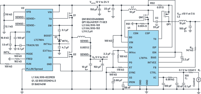
Figure 1. Electrical schematic of bipolar, bidirectional, 2-terminal power supply: VIN = 5 V to 24 V, VOUT = ±10 V at 3 A
Most electronic systems depend on power voltage rails that are either positive or negative, but a few applications require individual rails that can be both. In these situations, positive or negative power is supplied by the same terminal—that is, the output voltage of the supply can be adjusted through its entire voltage range, smoothly transitioning across polarity. For instance, some automotive and audio applications require, in addition to traditional voltage sources, power supplies that can function as a load and sinking current from the output terminals. Regenerative braking in automotive systems is one example. Single terminal, bipolar power supplies are documented, but solutions that can operate during input voltage drops, such as cold crank conditions, while continuing to provide bidirectional functionality are not.
Bipolar, bidirectional power supply circuit
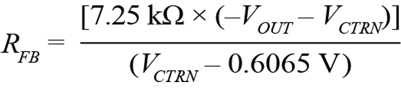
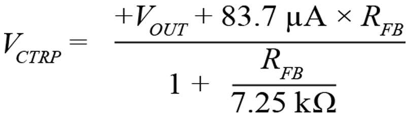
Figure 1 shows a 2-stage power supply, which centers around a 4-quadrant controller (stage 2), U1. This 4-quadrant converter is fed by an intermediate bus converter, VINTER (stage 1), supplying an output voltage in a min-max range of 12 V to 24 V, nominally 12 V to 16 V, matching the nominal voltage range of the standard automotive battery rail. The output of the complete 2-stage converter is ±10V delivering a 3A current to the load. The output voltage is controlled by the voltage source CONTROL signal at the CTRL pin of controller U1.
The low-pass filter CF, RF alleviates sharp changes in control voltage. The power train includes two MOSFETs, N-channel QN1, and P-channel QP1; two discrete inductors, L1 and L2; and an output filter. The choice of two discrete inductors instead of a single coupled inductor extends the range of suitable magnetics and allows the use of previously approved and tested chokes. The output filter is composed exclusively of ceramic capacitors because of the dual polarity nature of the output.
The input voltage range of the full 2-stage converter is 5V to 24V, to cover cold cranking voltage drops in automotive electronics and brownouts in industrial applications. The boost converter (stage 1), based on controller U2, maintains the voltage of the intermediate bus at or above 12 V whenever the converter is enabled. The power train of the boost converter includes inductor L3 and MOSFETs Q1 and Q2. The 2-stage arrangement allows normal operation of the downstream 4-quadrant converter to deliver ±10V to the load at all operational conditions.
How it works
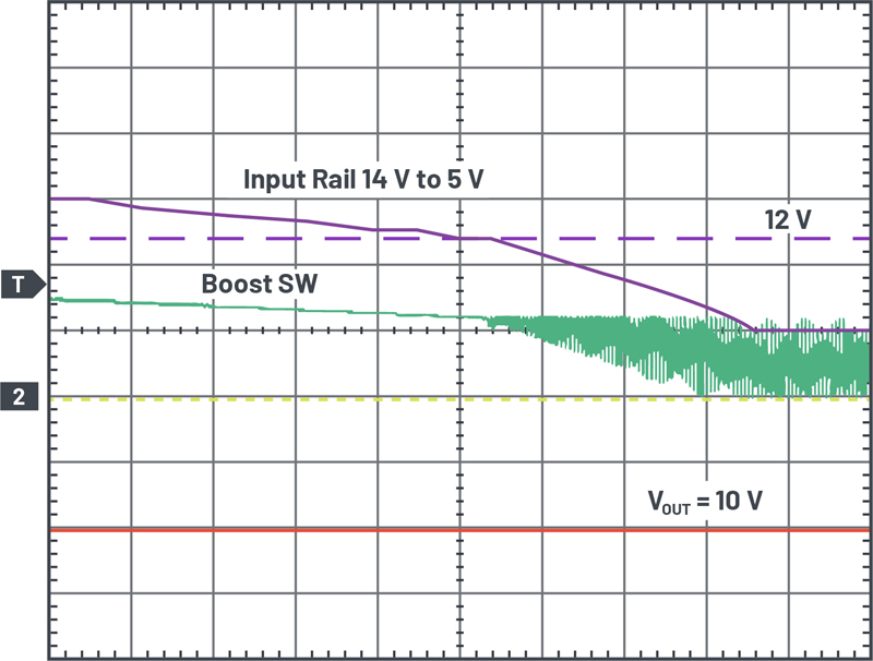
The oscillogram in Figure 2 shows the circuit of Figure 1 in action. When an input voltage is applied at VIN, the boost converter regulates its output, VINTER, to 12V if the input falls below this level. If VIN exceeds the 12V typical for a nominal 12 V automotive rail, then the boost converter enters Pass-Thru mode or wire mode. In this mode, the top MOSFET Q1 is enhanced at 100% duty cycle, always on operation, so no switching occurs — the voltage, VINTER, applied to a 4-quadrant converter remains relatively stable at a level equal to VIN.
Click image to enlarge
Figure 2. Waveforms showing VIN dropping from 14 V to 5 V. VIN = 5 V/div, VOUT = 5 V/div, boost SW = 10 V/div, and the time scale is 200 µs/div
This approach greatly increases system efficiency over a typical 2-stage device (namely, a boost converter followed by buck/inverting). This is because efficiency in Pass-Thru mode, where the system will spend most of its time, can be near 100%, essentially turning the power system into a single-stage converter. If the input voltage drops below the 12 V level — for example, during a cold cranking event — then the boost converter resumes switching to regulate VINTER to 12 V. This approach allows the 4-quadrant converter to deliver ±10 V, even when facing sharp drops of the input voltage.
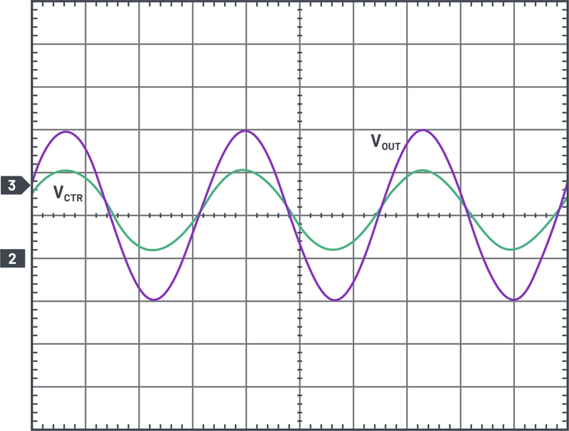
When the control voltage is at its maximum — in this case, 1.048V — the converter output is +10 V. If the control voltage is at its minimum (100 mV), the converter output is –10 V. Control voltage vs. output voltage is shown in Figure 3, where the control voltage is a 60 Hz sinusoidal signal frequency with a peak-to-peak amplitude of 0.9048V. The resulting converter output is a correspondingly 60Hz sinewave with a peak-to-peak amplitude of 20V. The output smoothly changes from –10 V to +10V.
Click image to enlarge
Figure 3. Waveforms of sine wave output as function of the sine control signal. VCTRL= 0.5 V/div, VOUT = 5 V/div, and the time scale is 5 ms/div
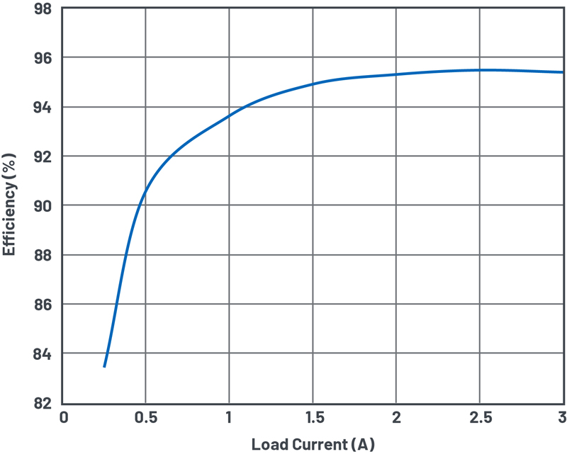
In this mode of operation, the 4-quadrant converter regulates the output voltage. The output voltage is sensed by U1 through the resistor RFBat its FB pin. The voltage at that pin is compared to the control voltage, and from that comparison, the converter’s duty cycle — that is, the gate signal on QN1 — is adjusted to keep the output voltage in regulation. If VINTER, CONTROL, or VOUT changes, the duty cycle is modulated to regulate the output accordingly. MOSFET QP1 switches in sync with QN1 for synchronous rectification to further maximize efficiency, as shown in Figure 4.
Click image to enlarge
Figure 4. Efficiency vs. load current
Sinking current
This 2-stage regulator can operate as a current source or a current sink. In current sink mode, current and power flow in reverse from the output, VOUT, to the input, VIN. This is important for automotive electronics and some audio systems. For the purposes of settling on verbiage when describing this mode, VOUT will now be referred to as the input and VIN will now be referred to as the output. Furthermore, this article only considers applications where VINTER bus voltage is equal to or greater than the minimum 12 V.
During reverse current flow, the 4-quadrant converter regulates output current that passes from VOUT to VIN; the converter does not regulate voltage in this mode. The 4-quadrant controller senses output current as the voltage drop across the sense resistor, RS2 in Figure 1, and regulates its duty cycle to keep this voltage drop at a set value, 50 mV, for this solution.
As a 4-quadrant converter generates voltage on the VINTER bus that exceeds the specified minimum, the boost converter enters Pass-Thru mode with top MOSFET Q1 always on and delivers the preset value of the output current to VIN (load) terminals with the smallest losses possible.
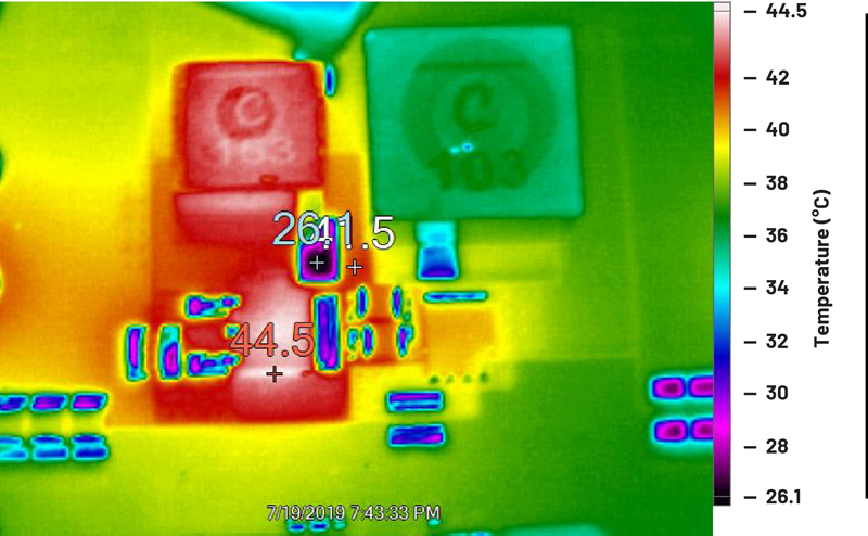
This mode of operation was benchtop verified and tested. To do so, the VOUT of the circuit in Figure 1 was connected to a lab power supply set to 12.5 V and the VIN to an electronic load, with the current through the converter set to 4.5 A. The thermal image of the 4-quadrant converter is shown in Figure 5.
Click image to enlarge
Figure 5. Thermal image of the 4-quadrant converter power train in load (reverse current) mode. A 4.5 A current flows from VOUT terminals to VIN from a 12.5 V source at VOUT
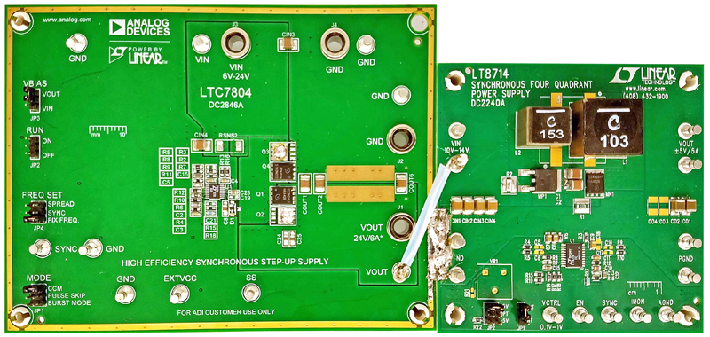
Figure 6 shows a photo of the converter itself, composed of two demo circuits from ADI soldered together: namely an off-the-shelf DC2846A boost converter demonstration circuit and the DC2240A 4-quadrant converter democircuit.
Click image to enlarge
Figure 6. Photo of the test fixture produced by soldering together two off-the-shelf demo boards from ADI. On the left, LTC7804 (DC2846A). On the right, LT8714 (DC2240A)
Component selection and calculations
The two controllers selected for this application were chosen for high performance, efficiency, and ease of use in their relatively specialized functions. The Power by Linear LT8714 is an easy to use 4-quadrant controller, featuring high efficiency synchronous rectification. The LTC7804 synchronous boost converter includes an internal charge pump, providing an efficient, switching free, Pass-Thru, 100% duty cycle mode of operation.
What follows is a formulaic analysis of stresses on the power train component and preliminary components selection. For deeper understanding and details of functionality, please refer to the LTspice models for these devices.

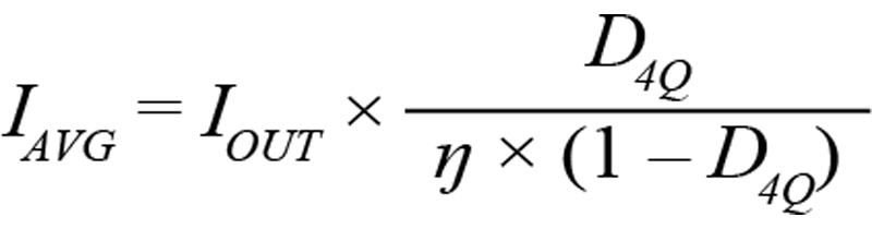
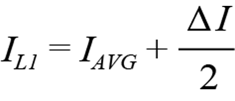
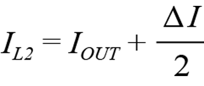
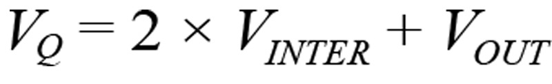


*Q1, Q2 voltage stress is defined by the maximum value VINTER or VIN