Designing Multi-Phase Converters for High-Current Applications

Powering the core rails of high-end field-programmable gate arrays (FPGAs) and application-specific integrated circuits (ASICs) requires high current as well as precise transient control.
Figure 1: Total Current Ripple for 4-Phase Application
In recent years, the rapid advancements in FPGAs, ASICs, and related systems have necessitated significant updates to power delivery regulations to address the increased complexity. These designs demand a delicate balance between efficiency, dynamic response, and the size and power loss of MOSFETs.
The most commonly used method to meet these requirements is to place multiple power supplies in parallel. This method distributes current equally between these power supplies (also called phases), which delivers the required power more easily and efficiently. A phase difference can be set between each power supply branch to further improve performance, thereby reducing the overall current and voltage ripple. However, this process can be complex since phases must be distributed equally, and the current must be balanced through all phases.
To meet the low-voltage, high-current demands of FPGA and ASIC core rails, and to manage precise transients’ control, power systems are now operating at higher frequencies using multi-phase power solutions.
For simplification, power modules such as the MPM3698 and MPM3699 implement advanced multi-phase control methods, including automatic interleaving and phase-shedding. This article will describe the design process for multiple-phase converters and explain the key aspects of multiple-phase power supply design.
FPGA and ASIC Design Requirements
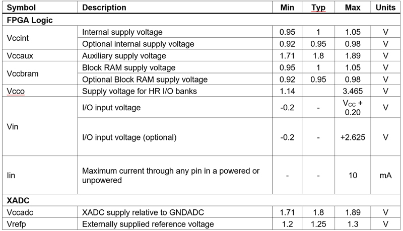
One of the most important criteria to consider while developing a power supply for FPGAs and ASICs is the voltage requirements for different power rails. For a generic voltage rail in FPGAs and ASICs, the default value for the input voltage (VIN) is 12V, the output current (ITDC) is 180A, and the output voltage (VOUT) is 1.2V. Table 1 shows the voltage requirements for a common FPGA; in this scenario, a sample of the Spartan 7 FPGA was used.
Click image to enlarge
Table 1: Recommended Operating Conditions for Spartan-7 FPGA (1)
Note:
1) The information for this table was presented in Mouser’s datasheet for Spartan-7 FPGAs Data Sheet: DC and AC Switching Characteristics
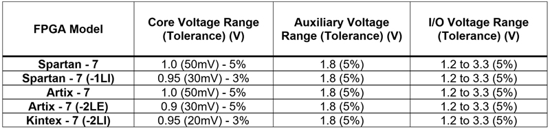
Table 2 shows the information for the core/aux and input/output voltages for different FPGAs currently presented on the market. The data listed in the table was obtained from the datasheets of the specific FPGA models listed in Column 1.
Click image to enlarge
Table 2: General FPGAs Comparison (2)
Note:
2) The information for this table was presented in Power Electronics News article titled Powering Your FPGA Applications
Both tables depict that voltage regulations are strict and that the designed power supply must provide precise voltage characteristics, since the tolerance is nearly ±3% in most modern cases. One of the possible ways to achieve these regulations is to use the multi-phase power supply method.
Multi-Phase Power Supply Method
A system’s fundamental frequency is effectively multiplied by the number of used phases. This increases the ripple frequency at the output, which results in a higher current capability with a smaller board space and lower output capacitance.
A buck converter used in ASIC and FPGA applications must have a fast transient response, meaning that it must be able to quickly transfer energy from the input to the output. By powering the load using parallel converters, each branch operates with an equal phase shift. This reduces the steady state voltage ripples and the input and output RMS currents, so the solution requires less input and output capacitance.
Using this method, it is possible to reduce the current ripple effectively and enable the use of smaller inductors, which also reduces transient voltage spikes. According to the frequency multiplication effect, the ripple’s amplitude is divided by the N number of branches (phases), and its frequency is N times larger. For example, a 4-phase application incurs a total inductor current ripple (IOUT = IO1 + IO2 + IO3 + IO4) that is four times smaller than the individual phase, and a ripple frequency that is four times larger than the individual phase (see Figure 1).
Challenges of a Multi-Phase Converter
Multi-phase converters are key for delivering high power levels with very fast response times. However, in applications such as FPGAs and ASICs, the power required by the system varies greatly. MPS provides both options: discrete and module solutions. However, modules are easier to design, consume less board space, and — when compared to discrete solutions — modules consist of three DrMos with a controller and three inductors, which significantly reduces design complexity. For instance, during peak processing loads, the output current demand may surge to 100A. Conversely, during idle or low-load periods, the current could drop significantly to 10A.
Additionally, modules bring other benefits such as current sharing, phase interleaving, the introduction of power delivery networks (PDNs), and optimization of input/output capacitance.
Multi-Phase Configuration Set-Up
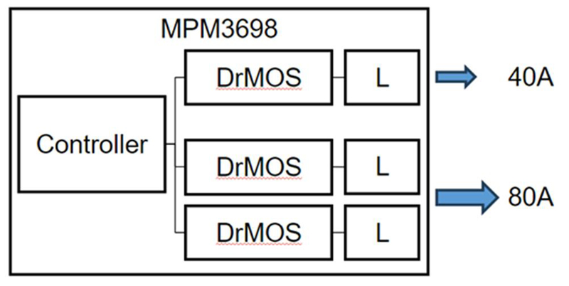
The MPM3698 is a fully integrated, single peak 120A or dual peak 80A + 40A power module with a digital interface. It integrates a VR14-compatible, dual-loop, digital multi-phase controller, as well as three sets of driver MOSFETs and inductors. The MPM3698 features MPS’s proprietary, digital, multi-phase nonlinear control scheme to provide ultra-fast transient response with minimal output capacitance.
Each phase of the MPM3698 can provide up to 40A of peak current and 30A of continuous current. The outputs of the three phases can be paralleled to provide up to 120A of peak IOUT, or 90A of continuous IOUT.
Figure 2 shows the internal set-up for the MPM3698. Each MPM3698 module consists of three DrMOS and a controller, which results in a total 120A of IOUT.
Click image to enlarge
Figure 2: MPM3698 Internal Set-Up
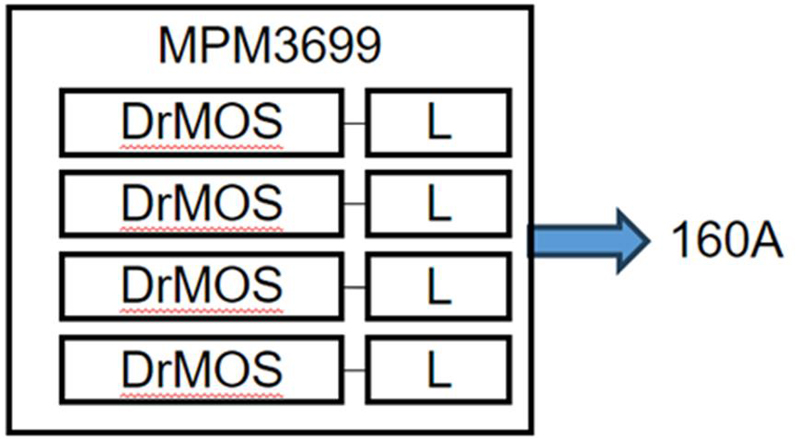
Implementing additional modules — such as the MPM3699 — to act as an external DrMOS through the PWM controller connection allows for more phases than the existing configuration that only uses the MPM3698. With the MPM3699 power module, IOUT can reach 560A or greater.
The MPM3699 is designed with four internal DrMOS modules, allowing it to produce up to 160A of IOUT. Figure 3 shows the MPM3699’s internal set-up.
Click image to enlarge
Figure 3: MPM3699 Internal Set-Up
MPM3698 Load Transient Test
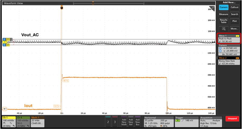
The output voltage tolerance and stability during load transients are one of the most important parameters for FPGA and ASIC applications. For the load transient test, the total number of output capacitors is 47, with each capacitor being 47µF, resulting in a total of 2.2mF of MLCC capacitance. Additionally, four POSCAPs are used, with each capacitor being 330µF. This results in a total of 1.32mF of POSCAP capacitance.
The load transient test conditions involve a 12V VIN, which is converted to 0.85V at the output, and a maximum current of 60A, which is divided across two phases and ranges between 0A and 60A. This test showcases the system’s impressive transient response, with an output voltage (VOUT/AC) that remains within a tolerance of ±3% (or ±30mV) (see Figure 4). This is a standard requirement for the VCORE rail of FPGAs.
Click image to enlarge
Figure 4: Transient Test (1 Module, 2 Phases, Load Transient = 0A to 60A, with Peak-to-Peak Voltage within ±30mV Tolerance)
From the load transient analysis, it is clear that the MPM3698 fulfills strict regulatory requirements for the transient response for FPGAs core voltage rail, having the peak-to-peak value of 50.36mV for 0.85V VOUT, which is within 3% (or ±30mV) of the I/O voltage tolerance.
Conclusion
Due to the demanding and strict requirements for the power supply of FPGAs and ASICs, multi-phase buck converters have become essential for powering high-performance devices. Implementing a multi-phase approach can deliver low voltages with high-current capabilities. Multi-phase power supplies offer fast transient response, with the ability to maintain tight voltage regulation, within ±3% tolerance, which is essential for the core and auxiliary power rails of modern FPGAs and ASICs.
The MPM3698 features MPS’s proprietary, digital, multi-phase nonlinear control scheme to provide ultra-fast transient response to the load transient. In addition, it features design simplicity and flexibility in a small solution size. By distributing power across multiple phases, devices such as the MPM3698 and MPM3699 improve efficiency, reduce thermal stress, and require smaller input and output capacitance. For excellent interleaving and high performance, explore MPS’s catalog of power modules.