Designing Robust Discharge Switches for High-Voltage Battery Management Systems
The transition to higher-voltage battery platforms (72V and above) is accelerating across e-mobility, industrial equipment, and battery-powered systems
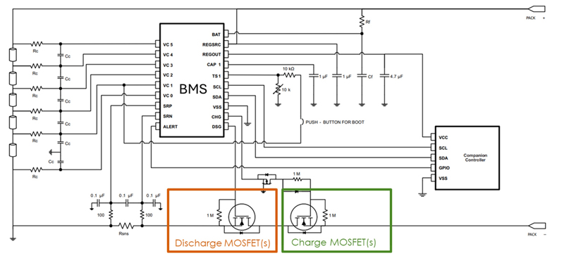
Figure 1: Simplified BMS topology showing charge and discharge MOSFETs
While higher-voltage battery platforms improve efficiency and reduce current, they also introduce a more demanding challenge: safely managing fault energy during abnormal conditions.
External short circuits in high-voltage systems can generate extreme currents within microseconds, placing the battery management system (BMS) in a critical protection role. At the center of this protection is the discharge MOSFET, which must interrupt fault current before damage propagates through the system.
This article examines the unique short-circuit challenges in high-voltage BMS designs and how MOSFET selection, particularly short-circuit withstand capability (SCWC), directly impacts system safety, reliability, and design complexity.
The Shift Toward High-Voltage Battery Architectures
Battery-powered systems are increasingly moving toward higher operating voltages to improve efficiency, reduce thermal losses, and increase power density. Platforms at 72V and above are now common in light electric vehicles, drones, and professional power tools.
Fundamental electrical relationships drive this shift. Increasing voltage reduces current for a given power level, lowering I²R losses, simplifying thermal management, and enabling smaller conductors and interconnects. The result is a lighter, more compact, and more efficient system.
However, higher voltage systems also store more energy and generate substantially higher fault currents under abnormal conditions. During an external short circuit, current can rise to several thousand amperes within microseconds, placing substantial stress on BMS protection components, particularly the discharge switch.
Why the Discharge MOSFET Is the Critical Protection Element
A battery management system must protect lithium-ion packs against overvoltage, undervoltage, overcurrent, and thermal runaway. At the heart of this protection are the charge and discharge MOSFETs, highlighted in Figure 1, which control when the battery is connected to the load and charger.
Although both switches are essential, the discharge MOSFET plays a uniquely critical role during external short-circuit events. Because of the body diode orientation, the charge MOSFET cannot block a direct Pack+ to Pack− short circuit. As a result, the discharge MOSFET alone is responsible for interrupting the fault current.
When a short occurs, the BMS must detect the condition and command the discharge MOSFET to turn off, typically within tens of microseconds. During this brief interval, the device must withstand extremely high current and associated thermal stress. If the MOSFET fails before successfully interrupting the current, the result can be uncontrolled energy release, leading to severe damage or catastrophic battery failure.
Unlike many other protection elements, the discharge MOSFET represents a single point of failure during external short-circuit events. If the device cannot survive long enough to turn off, no downstream protection mechanism can prevent uncontrolled energy release. This makes the discharge MOSFET one of the most safety-critical components in a high-voltage BMS.
The Short-Circuit Withstand Challenge
Short-circuit withstand capability (SCWC) is a time-dependent survivability metric that defines whether a MOSFET can remain functional long enough for the BMS to detect a fault and initiate turn-off.
In practical systems, protection circuits require tens of microseconds to respond. During this interval, the MOSFET must simultaneously sustain high current and rising junction temperature without entering thermal runaway. Devices with insufficient SCWC may fail before protection circuitry can act, effectively bypassing the intended safety mechanism.
Historically, MOSFET design has involved a trade-off between low RDS(on) and short-circuit robustness. As battery voltages increase and safety margins shrink, this trade-off becomes more difficult to manage at the system level.
Characterizing Short-Circuit Withstand Capability
SCWC is characterized using controlled short-circuit testing, as shown in Figure 2, where devices are subjected to increasing current pulses until failure occurs. Unlike static datasheet parameters, this approach captures the dynamic interaction between current density, thermal rise, and turn-off behavior.
The resulting failure current provides a practical measure of fault energy tolerance and directly informs how many MOSFETs must be paralleled to meet system protection requirements. A higher failure current allows designers to use fewer MOSFETs in parallel to meet a given short-circuit requirement, reducing board area, bill of materials, and overall complexity.
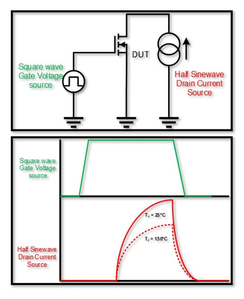
Click image to enlarge
Figure 2: Short-circuit withstand testing setup using a controlled current pulse and gate turn-off event
Quantitative Comparison: Breaking the Trade-Off
In comparative testing of 150V, 2.5mΩ MOSFETs in the TOLL package, the SuperQ device sustained a peak short-circuit current of 641A, compared to 612A for a competing device with similar ratings, representing a 29A improvement in SCWC.
When short-circuit current is evaluated alongside RDS(on), the performance difference becomes more apparent. Rather than trading one parameter for the other, the higher-performing device occupies a favorable region where low conduction loss and high short-circuit robustness coexist. From a BMS design perspective, this margin is highly consequential. Higher SCWC extends the allowable protection response time and reduces the number of devices required in parallel to safely interrupt fault current.
Structural Drivers of Short-Circuit Robustness
The observed improvement in short-circuit performance is closely tied to MOSFET cell design. Structural features such as mesa width and metal contact geometry play a critical role in determining current density, heat spreading, and transient energy absorption.
Wider mesa regions for SuperQ MOSFETs, as illustrated in Figure 3, provide a larger conduction area, allowing current to be distributed more evenly across the silicon. This improved current distribution delays the onset of localized thermal runaway, the primary failure mechanism during short-circuit events. In contrast, aggressively scaled mesas, used in some designs to minimize RDS(on), can limit current-handling capability and reduce SCWC.
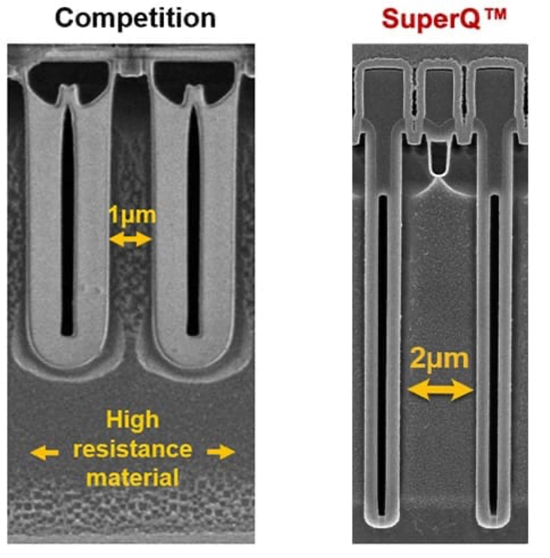
Click image to enlarge
Figure 3: Comparison of MOSFET cell structures
By optimizing mesa width and contact design, it is possible to improve short-circuit robustness without sacrificing conduction efficiency. This demonstrates how silicon architecture can improve robustness without sacrificing efficiency, even within mature CMOS-compatible processes.
System-Level Implications for BMS Designers
From a system designer’s perspective, improved SCWC translates directly into practical benefits. In a typical 80V battery pack, higher short-circuit robustness can reduce the number of MOSFETs required in parallel to interrupt fault current safely. Instead of four or five devices, only two or three may be needed to meet the same safety requirements.
Reducing the number of parallel devices lowers bill of materials cost, simplifies PCB layout, and reduces parasitic resistance and inductance. It also improves current sharing and thermal balance, further enhancing reliability.
In addition, reducing the number of parallel MOSFETs simplifies gate-drive design and improves switching consistency during fault conditions, where timing mismatches between devices can otherwise introduce additional stress.
Lower RDS(on) provides additional advantages by minimizing conduction losses under normal operating conditions. This improves overall system efficiency, reduces heat generation, and can extend battery runtime.
Taken together, these benefits demonstrate that discharge MOSFET selection influences not only safety but also cost, efficiency, and system complexity.
Implications for Next-Generation Battery Systems
As battery voltages continue to rise and application requirements become more demanding, traditional MOSFET selection criteria are no longer sufficient. Designers must evaluate short-circuit robustness with the same rigor applied to conduction losses and thermal performance.
Short-circuit withstand capability is emerging as a defining parameter for high-voltage BMS designs, particularly in applications where safety, reliability, and compactness are critical. Devices that combine high SCWC with low RDS(on) enable simpler, more robust systems and provide greater design margin against worst-case fault conditions.
Conclusion
As battery voltages continue to increase, the role of the discharge MOSFET is evolving from a simple switching element to a critical safety component.
Evaluating MOSFETs based solely on on-resistance is no longer sufficient. Short-circuit withstand capability must be considered as a primary design parameter, as it directly determines whether protection mechanisms can function as intended.
By selecting devices that combine low conduction loss with high SCWC, designers can reduce system complexity while improving fault tolerance, ensuring that high-voltage battery systems remain both efficient and inherently safe.