Author:
Oliver Haeberlen, Fellow Power Semiconductor Devices & Technologies, and Tim McDonald, Senior Consulting Advisor to the CoolGaN™ Development Program, both at Infineon Technologies
Date
02/22/2023
 PDF
PDF

Click image to enlarge
Figure 1: Infineon’s four-step qualification plan for CoolGaN™ devices
Introduction
Silicon semiconductor technology has evolved considerably over the past 50 years, during which time, multiple failure modes affecting device reliability have been discovered, researched, and addressed.
This has led to the development of models and equations for failure modes like time-dependent dielectric breakdown (TDDB), bias temperature instability (BTI), electromigration (due to high current density in conductors), and corrosion (due to humidity and bias), which can be used to predict silicon device behavior and reliability in the field.
However, while many of the models can also be applied to devices constructed using more recently developed Gallium Nitride (GaN) technology, the differences in the crystalline structures of both technologies mean existing silicon models used to qualify GaN devices need to be more comprehensive. Investigating the stresses endured by GaN devices in their intended applications provides a better insight into their expected operating lifetime to improve their quality and robustness.
Infineon has devoted substantial resources to this analysis, which has enabled it to determine what changes must be introduced to the development and reliability qualification processes. This article describes the methodology it has used to develop a comprehensive and effective four-step qualification plan (Figure 1), which it now uses for its CoolGaN™ devices and its products. At the same time, it will discuss how to ensure the safe and reliable operation of GaN devices.
The first step in the qualification plan is understanding the stresses a GaN device experiences while operating in a specific topology. A complete application profile includes relevant system-level requirements, which (amongst others) are:
• output power vs. time,
• the length of time operating at different temperatures and relative humidity,
• hard or soft-switching.
Telecom rectifier (AC-DC) sockets represent a good use case for GaN device qualification as they can experience stressful operating conditions; they are required to operate for a long time in the field with widely varying (and sometimes extreme) ambient temperatures and humidity levels.
While these make this an excellent application for GaN device qualification, this approach can also be applied to similar applications using the same power conversion topologies but which experience more benign conditions (e.g., server or TV power supplies). At the center of an application profile is a table where device stress modes (voltage and current) are detailed as a function of temperature and humidity (Figure 2).

Click image to enlarge
Figure 2: Operating conditions for the telecom rectifier application profile
When considering the application conditions, it is also important to capture any substantial differences in the spike, or average voltage (VDS) applied to the device.
The second step is to generate a profile of quality requirements. This involves establishing the following:
• A general description of the application,
• Customer target lifetime (varies depending on the application),
• The maximum allowable cumulative failure rate,
• Definition of parametric drift limits, e.g., for the required electrostatic discharge (ESD) rating,
• Requirements for humidity in the operating environment,
• Moisture sensitivity level (MSL) rating.
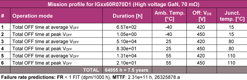
For example, the requirement for the telecom rectifier market is a 15-year lifetime with a failure in time (FIT) rate of 1 FIT (that equates to one failure per billion device hours).
While developing its CoolGaN™ devices, Infineon performed a thorough reliability investigation of GaN-specific failure modes. These are either intrinsic (due to inherent wear-out of device structure and materials) or extrinsic (due to defectivity or very high process variability).
Reducing the number of defects and process variations to eliminate extrinsic failures and tighten the variability in the intrinsic failure distributions is a key task of technology development. Infineon’s advanced process capabilities and analysis tools effectively mitigate these variations. Early reliability investigations use tools such as a Weibull plot which takes time to failure (TTF) data and graph the fraction of a failed sample (y-axis) versus time under stress (x-axis).
The Weibull plot on the left side of Figure 3 shows failures over time (on a logarithmic scale), where a small fraction of the devices (circled group) were early failures compared to the majority of devices failing at much later times. Each data point on the graph represents when an individual device failure occurred (x-axis) and the cumulative fraction of the population that failed before and including that device (y-axis). The subset of early-failing parts indicates different failure mechanisms, typically due to either defectivity or a wide process variation (or potentially a combination of both), and is reflected by a low shape factor of the distribution (Beta <1). The plot on the right side of Figure 3 shows a steep Weibull distribution with a high Beta number indicating a pure intrinsic failure mode with a single failure mode and low process variability typical for CoolGaN™ devices.

Click image to enlarge
Figure 3: A Weibull plot showing individual failures vs. time (on a logarithmic scale)
Reliability investigations aim to discover the intrinsic and extrinsic failure mechanisms for each type of stress and which test parameters like voltage, current, or temperature mainly affect the lifetime. Based on those investigations, degradation models for all relevant intrinsic mechanisms and, ideally, also extrinsic mechanisms are generated to predict device lifetime and failure rates. Those models are also needed to derive proper electrical screening conditions to lower the early “infant mortality” failures to the required ppm level.
Examples of degradation models are the Arrhenius equation for any temperature-activated degradation characterized by its activation energy or the voltage acceleration described in the most conservative case by the so-called Linear-E model for field-assisted bond breakage. It describes the exponential dependency of the lifetime from the electric field in the device and is used, for example, in modeling the DC drain bias lifetime.
Some of the most critical failure mechanisms for GaN devices that do not occur in silicon power FETs include:
DC drain bias lifetime
While silicon devices are also susceptible to DC drain bias failure (requiring high-temperature reverse bias – HTRB – testing to be performed), the difference with GaN HEMT devices (when tested at accelerated voltage and temperature conditions) is that they exhibit a strongly voltage-dependent failure rate and lifetime, which can be modeled using a Weibull plot together with the corresponding acceleration models for voltage and temperature.
Switching Safe operating area (SOA) failure mode and model
This is also known as dynamic high-temperature operating life (DHTOL). Like other semiconductor manufacturers, Infineon publishes long-term application switching data, demonstrating stable device operation (measured as steady case temperature) in hard-switching (boost) applications over time durations ranging from 1,000 to 3,000 hours, using a test platform that allows accelerated testing at the voltage and current levels which exceed design specifications. Based on highly accelerated test-to-fail runs with different voltages and switching currents, lifetime models have also been extracted to ensure that application requirements are met.
Dynamic RDS(on)
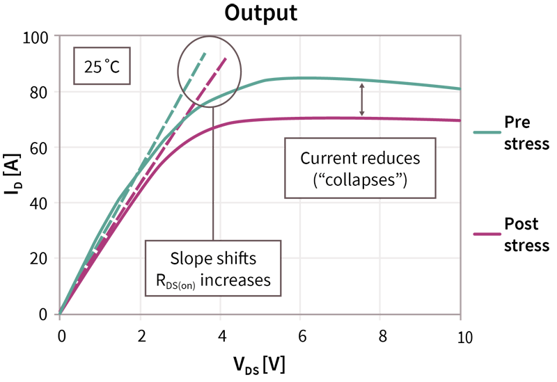
High electric fields in GaN devices can cause charge to be trapped in various regions of the device depending on device design and material quality. Such electric fields can be present during off-state or in combination with hard switching transitions during which high electric fields are combined with high current. Those trapped charges affect the device output characteristics, and since they have a finite relaxation time, the temporary increase of RDS(on) is called dynamic RDS(on).
Figure 4 shows the output characteristic (I-V) for the initial (pre-stress) condition (solid blue line). The tangent or slope of this curve shown (the dashed blue line) corresponds to the initial value of RDS(on). When a DC bias is applied, or the device is exposed to a hard switching event, the output curve changes slope (corresponding to an increase in RDS(on)), and the peak output current reduces. Stable dynamic RDS(on) is an essential criterion for reliable operation in application circuits.
Click image to enlarge
Figure 4: RDS(on) and saturation current values shift between those measured before (blue dash) value and post (red dash) application of DC bias or hard switching stress
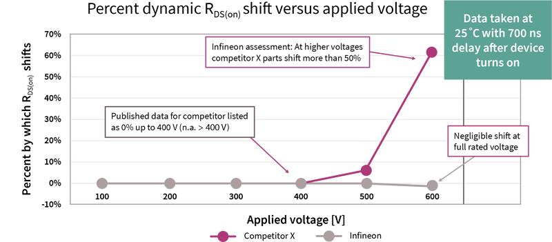
Infineon CoolGaN™ devices exhibit very low dynamic RDS(on) (measured at 20 A under hard-switching conditions). This parameter varies only slightly (even up to the rated voltage of 600 V) when compared to a competitor device, which exhibits a strong increase in dynamic RDS(on) at voltages down to 400 V (Figure 5).
Click image to enlarge
Figure 5: Dynamic RDS(on) as a function of drain voltage
While Infineon has developed four GaN degradation models, only two are considered here for brevity: DC drain bias and switching SOA. With reference to an application profile, these two models can be used to determine if a GaN device will operate for the required lifetime and quality level.
DC drain bias model
Consider the application profile for a 2.5 kW AC-DC power converter for use in telecom systems, using a CCM totem pole hard-switching configuration running at 65 kHz to perform power factor correction (PFC). The DC-DC section uses an LLC (soft-switching) topology.
As the system can be installed in potentially extreme environments, a wide temperature range is required (ambient temperature varies between -27.5°C and 72.5°C in the box/cabinet of the system) with a fraction of the operating time at each temperature. The average voltage output of the PFC is 400 V with a turn-off spike/peak between 410 V at standby and 460 V at the 80-100 percent output power condition.
The system has a 100 percent operating time with a 15-year lifetime but operates between standby and 80-100 percent load with a given load profile. The load current varies between 1.5 A at standby and 18 A at 80-100 percent load condition. Using bias and time data from the application profile as inputs (Figure 6), the DC bias degradation lifetime model estimates a cumulative failure rate of less than 1 FIT for the telecom rectifier application.
Click image to enlarge
Figure 6: Estimating the failure rate of a GaN device in a telecom application using the DC bias model
Checking the telecom AC-DC application against the switching SOA model and rating
Infineon provides repetitive SOA (switching) curves (based on the DHTOL/dynamic switching degradation model) in the datasheets for its CoolGaN™ devices that can be compared to a required application profile.
For example, Figure 7 shows the curves for the CoolGaN™ GIT HEMT 600 V IGT60R070D1, a 70 mΩ, 600 V-rated GaN device that matches the application requirements of the telecom rectifier. The horizontal axis represents the DC link voltage, and the vertical axis the maximum allowed repetitive peak switching current, including the current overshoot ΔI = Csw * dV/dt induced by the total switch node capacitance.
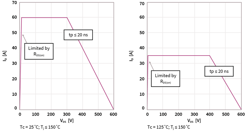
Figure 7: Repetitive safe operation area curves depict the allowable I-V operating area to avoid failure due to dynamic switching of CoolGaN™ devices
GaN and silicon devices differ considerably in how they operate, which means the models and equations used to predict silicon failures are insufficient to predict the long-term behavior of GaN devices. This has necessitated developing a new approach to predicting the behavior of GaN devices in the field over their working lifetime.
Investing significant resources to understand potential failure mechanisms and how to model them has enabled Infineon to develop a four-step plan, which it now uses to ensure its CoolGaN™ devices can meet the reliability requirements level required for a given application.
To find more information on how the pioneering quality of Infineon’s highly efficient GaN technology ensures the highest standards visit our GaN technology website.
To browse the broad product portfolio offering some of the most reliable and performing solutions among all GaN HEMTs on the market visit our GaN HEMTs website.
References
[1] McDonald Tim, “Reliability and qualification of high-voltage CoolGaN™ GIT HEMTs,” Whitepaper, Infineon Technologies, April 2022 [Available online]