Innovative top-side cooling approach to reach the full potential of onboard charger designs
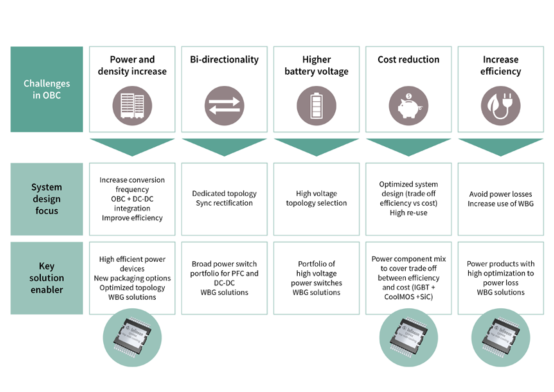
Figure 1: OBC design presents a number of challenges to power designers
Within the automotive industry, development and innovation continue at a rapid pace in almost all aspects of vehicle design, from the chassis to the powertrain, infotainment, connectivity, and automation. However, with the time taken to recharge electric vehicles (EVs) – especially in-journey – being cited as a significant inconvenience that is hampering adoption, the design of the onboard charger (OBC) is perhaps an area that is coming under more scrutiny than most.
As with most engineering challenges, designers are looking to advanced technology to provide the solution with modern Silicon Super Junction (SJ) technologies and wide bandgap (WBG) materials such as silicon carbide (SiC) and gallium nitride (GaN) being hailed as the solution. However, the semiconductor material can only be part of the solution. Without effective thermal engineering, no OBC design will ever reach its full potential in terms of power density and efficiency.
In this technical white paper, Infineon will consider the challenges facing OBC designers and look in detail at the role that semiconductor packaging plays in delivering a solution. An innovative approach to top-side cooling that supports an integrated suite of high-performance components for designers to select from will be discussed.
The challenge of OBCdesign for modern EVs
The role of the OBC is to convert AC power from the grid into a DC voltage that can be used to charge the traction battery. The OBC only performs this function while the vehicle is parked and connected via a charging cable. While the vehicle is moving, it is simply a weight that must be carried around; the size and weight of the OBC must be minimized to reduce its effect on the range – while still allowing for rapid and efficient charging. Another challenge is the rapid power class increase in the OBC. While 3.6 kW was state of the art a few years ago, in the near future we could talk for about three times higher power, i.e., 11 kW under the same space considerations.
There are five key challenges for OBC designers which interrelate with each other. The increase in power density is particularly important as this implies a reduction in size as well as weight which, in itself, will contribute to extending the range of the EV. Enhancing efficiency not only reduces the heat buildup within the OBC (which reduces size and increases power density due to reduced thermal management), but it also allows more energy from a finite grid source to be delivered to charge the traction battery, thereby reducing the effective charging time.
Traction battery voltages are increasing – the typical 400 V is becoming 800 V – primarily to reduce currents and the associated I2R losses in cabling when charging and when delivering energy to the traction motors.
The requirement for bi-directional operation is a further challenge for OBC designers. As EVs become more common, the pressure on the grid will increase significantly, especially as people are expected to recharge their vehicles at the same time (for example, in the evening after the daily commute). Electricity suppliers recognize that there is a significant amount of energy stored in EVs that could either be used to stabilize the AC grid or to power a single house at peak times to reduce peak demand. Moreover, the EV could act as a “house battery” when the AC grid fails (blackout scenarios). However, to do so, the OBC needs to be able to transfer energy from the traction battery as well as receiving it.
To address these challenges, the topology chosen will be important, as will the technology used – especially for the switching components. In most cases, WBG solutions will contribute significantly to providing the performance benefits needed.
However, while understanding the benefits offered by WBG technology, designers must also consider that improved thermal performance will play a crucial part in achieving these important goals.
Top-side cooling – overview and benefits
Given that the automotive environment contains many hazards for electronic assemblies, including dust, dirt, and fluids, most electronic systems in EVs are sealed for protection. This precludes forced air as a means of cooling and, therefore, thermal management generally involves conducting heat away from high power components to the liquid coolant in the EV.
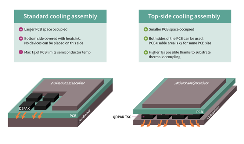
In general, the conduction path for high-power SMD components is downwards from the power component into the PCB, which is bonded to a cold plate. This is called “bottom-side cooling” (BSC). In challenging applications, the power components may be mounted on an insulated metal substrate (IMS) which improves thermal performance as it is a better conductor of heat than FR4 with thermal vias. However, BSC is always a compromise between thermal performance and PCB utilization.
Through innovative packaging, Infineon has developed the ability for discrete semiconductors and power ICs to be able to be top-side cooled (TSC). This option delivers a number of additional benefits, all of which are beneficial to OBC design and other similar applications.
In bottom-side cooling, a cold plate is typically attached to the bottom side of the PCB / IMS to dissipate heat. This precludes the placement of components on one side, which can reduce the power density by a factor of two. The semiconductor devices are thermally bonded to the PCB, which means that they will operate at the same temperature. As the Tg of FR4 is lower than the operating temperature of many modern power devices, they are unable to be used to their full potential.
Click image to enlarge
Figure 2: TSC permits double-sided component placement, allowing for a doubling of power density
With the cold plate bonded to the top side of the power components, these issues are addressed, allowing for components to be placed on both sides, and WBG devices are able to be used over their entire operating temperature range.
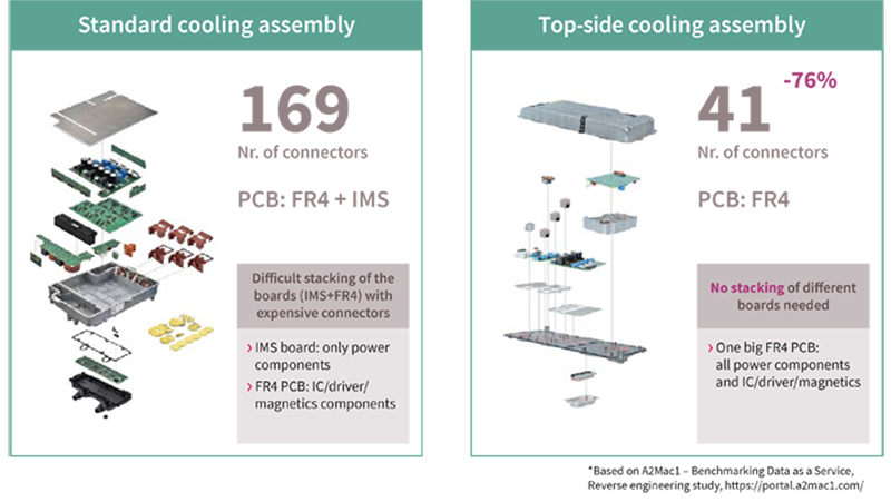
While an IMS can offer enhanced performance over FR4, it also introduces complexity. In fact, many IMS solutions become a multi-board assembly using IMS for the power devices only and FR4 for the drivers and passives. This introduces a significant amount of complexity in design and manufacturing. However, a recent teardown report showed that a real-world assembly of this type used 169 (!) connectors – while an equivalent top-side cooled design required just 41 [1].
Click image to enlarge
Figure 3: The simplicity of a TSC assembly typically removes up to 76 percent of the interconnect requirements1
Moving to a single board TSC design removed the cost and complexity of 128 connectors, as well as the reliability concerns associated with them. The cost of the IMS was eliminated, and, according to the teardown report, assembly costs were reduced by a third.
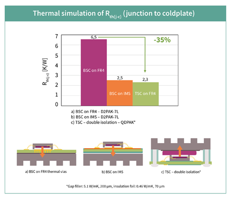
The critical parameter in thermal design is the thermal resistance between the semiconductor junction and the cold plate, as this defines the ability to move heat energy. Thermal simulation of TSC on FR4 shows that it is 35 percent better than bottom-side cooling on FR4 and shows a slight improvement in thermal performance over bottom-side cooling on IMS – with a significant cost saving.
Click image to enlarge
Figure 4: Despite costing less, TSC offers better performance than a bottom-side cooled IMS design
The thermal limitation on the FR4 itself is associated with this, which is a safety requirement. In a bottom-side cooled scenario, the MOSFET is bonded to the FR4, meaning that the temperature of the FR4 is very close to that of the semiconductor junction. The limitations put upon the temperature of the FR4 mean that the operating temperature of the MOSFET is restricted so that it cannot operate at its full potential. Within the TSC approach, there is no thermal bonding between the MOSFET and the FR4, so the MOSFET can operate at higher temperatures.
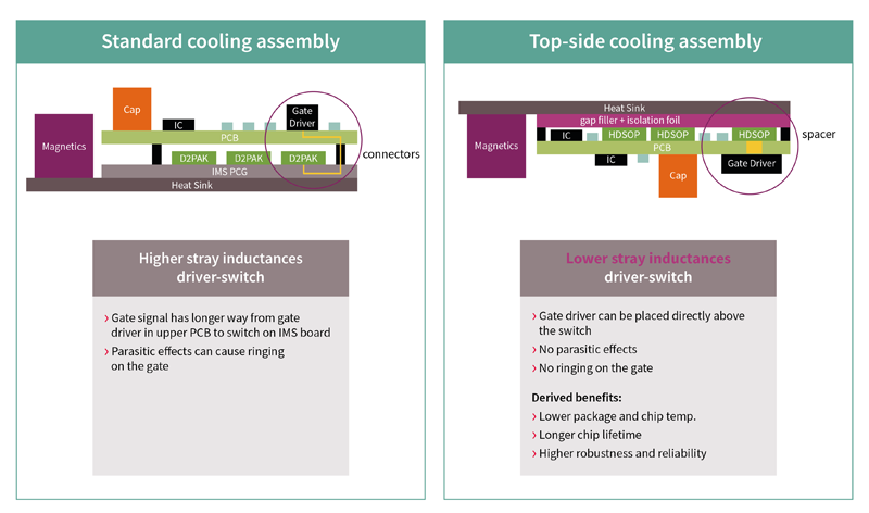
As the use of IMS normally involves using a separate FR4 PCB for the driver and passive components, there can be a significant distance between the gate driver and the MOSFET, which inevitably increases the parasitic effects that cause ringing.
Click image to enlarge
Figure 5: SMD power devices with top-side cooling allow for short gate traces, reducing the parasitics
As TSC allows all components to be placed on the same double-sided PCB, the driver can be placed directly below the corresponding MOSFET, significantly reducing parasitic effects due to the PCB. This enhances system performance, yields cleaner waveforms, and thus reduces the electrical stress on the power components.
Assembly considerations
As discussed above, a typical TSC assembly will generally be simpler than the equivalent bottom-side cooled approach, not least as there is a single board and significantly less interconnect that requires to be placed.
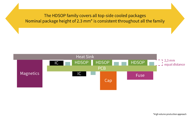
The heatsink is thermally attached to the heat-generating MOSFET packages on the top side of the PCB. Low profile components could also be placed on this side, while taller components being placed on the underside. In developing their HDSOP family, Infineon has ensured that every component has a nominal height of 2.3 mm. This uniform height greatly simplifies the cold plate and removes the need for machining, allowing more optimized heatsinks to be used even when different power semiconductor technologies are used in the same design.
Click image to enlarge
Figure 6: A uniform height for all HDSOP devices dramatically simplifies the design and assembly of the heatsink
Multiple options exist for thermally bonding the MOSFET packages to the cold plate. In general, the simplest approach is to place a single thermally conductive gap filler pad between the MOSFETs and heatsink. An optimized gap filler height gives the best thermal performance, provided that any voids in the gap filler are addressed. Also, the production line can be fully automatized when using liquid gap filler materials.
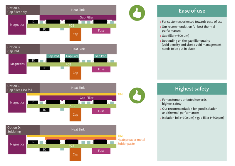
Click image to enlarge
Figure 7: A gap filler is the preferred thermal bonding approach, with the addition of an insulator for increased safety requirements
Although the gap filler is able to provide sufficient electrical isolation between the MOSFETs and the conductive heat sink, an additional isolation foil can be placed between the gap filler and heatsink to provide the appropriate level of electrical isolation without significant deterioration of the thermal performance for increased safety requirements.
Infineon’s QDPAK– an advanced TSC solution
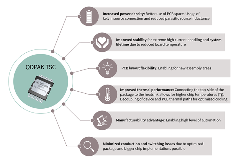
Infineon’s QDPAK devices are specifically designed to take advantage of the benefits of TSC, and a variety of features are offered to suit different applications. With a nominal footprint of 20.96 mm x 15.00 mm and a consistent 2.3 mm height throughout the series, the devices offer ease of assembly.
Since QDPAK devices are capable of dissipating high power and with multiple pins dedicated to the drain and source connections, they are ideally suited to a high current operation.A Kelvin source pin is provided for high levels of controllability and full load efficiency, enabling high frequency operation to achieve power density targets.. The symmetrical parallel lead layout ensures mechanical stability on the PCB as well as easy assembly and test.
Click image to enlarge
Figure 8:The TSC-capable QDPAK offers many manufacturability/assembly benefits
As standard, the QDPAK (PG-HDSOP-22-1) offers a creepage distance of 3.20 mm for a working voltage up to 450 V [2]), covering most applications in the sub-400 V battery classes. For more challenging applications, the HV QDPAK (PG-HDSOP-22-3 [3]) will offer a mold compound material class I and include a groove in the package that increases the creepage distance to 4.80 mm, enabling a 950 V working voltage.
Summary
While wide bandgap (WBG) semiconductor materials are occupying the headlines in the battle to achieve ever greater efficiency and power density from power solutions, effective thermal management has a significant goal to play in achieving electrical performance as well as reducing size, weight, and cost.
Innovative design of packages, such as Infineon’s QDPAK, allows for top-side cooling (TSC), where the heat flows through the top of the package via a thermal interface material directly to the cold plate. This approach offers many benefits, including better thermal performance than the equivalent IMS-based solution. The more straightforward construction eliminates multi-board assemblies, reducing component count and cost (especially for connectors). Consequently, performance is significantly improved, and assembly time and cost are reduced. The ability to use both sides of the board significantly improves power density while reducing parasitic elements in the system.
While TSC may seem ‘new’ and in many ways it is, the real beauty of this solution is that it uses tried-and-tested techniques such as gap fillers with/without thermal interface material to produce a solution that is elegant and, above all, reliable.
Make sure to navigate Infineon’s QDPAK webpage and learn more about our innovative top-side cooled SMD solutions for high power applications and their key features and benefits when combined with our latest high-voltage superjunction MOSFET and CoolSiC™ technologies.
[1] Based on A2Mac1 – Benchmarking Data as a Service, Reverse engineering study, https://portal.a2mac1.com/
[2] according to the DIN VDE 0100 / IEC 60664-1 standard with material class II
[3] For early samples availability please contact Infineon sales.