Operating conditions
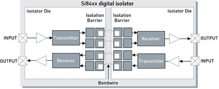
For more than four decades, optocouplers have been the "default" signal isolation device, but CMOS-based digital isolation technology has made available smaller, faster and more reliable solutions that have begun replacing optocouplers in many applications. Both classes of devices must provide signal transmission with galvanic isolation, often in harsh industrial environments and in the presence of strong electromagnetic fields, surges, fast transients and high noise levels. An optocoupler is a hybrid assembly that pairs a forward-biased light-emitting diode (LED) and a photodetector. The LED emits light in response to the incoming signal: the light passes through a transparent, electrically-insulating film or dielectric, and the detector recovers the signal and presents it at the output pins. The digital isolator's basic operation is similar to that of the optocoupler, except an RF signal replaces the emitted light. For example, Silicon Labs' digital isolator IC consists of two identical semiconductor die connected to form an RF transmitter and receiver separated by a differential isolation barrier. Data is transferred from input to output using simple on/off keying. When VIN is high, the RF carrier is transmitted across the isolation barrier. The receiver asserts logic 1 on VOUT when sufficient in-band carrier energy is detected.
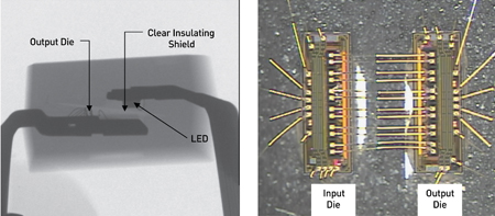
In an optocoupler (Figure 1a), the LED and output die are attached to a split lead frame and separated by a physical gap containing a transparent shield that reduces parasitic input/output coupling capacitance. Optocoupler cost and complexity increases with channel count, and isolation breakdown voltage is primarily determined by the package plastic mould compound. The 6-channel digital isolator (Figure 1b) contains two die fabricated in standard CMOS technology in standard IC packaging. Each die contains six isolator channels (transmitter, differential isolation barrier, and receiver circuit) and forms six complete isolator channels when connected. Unlike the optocoupler, the digital isolator channels occupy a very small die area, enabling cost-effective, high-channel-count isolation solutions.
Isolators must meet safety standards for robust galvanic isolation and be reliable enough to outlast the equipment in which they are installed. The designer must consider operating parameters such as common-mode transient immunity (CMTI), key timing parameters, and noise immunity characteristics such as EMI and RF susceptibility, and reliability concerns such as continuous working voltage and mean time-to-failure (MTTF). Safety insulation is the most critical aspect of an isolator, and insulation must be uniform; uniformity is a function of the insulator material and the fabrication process. The dielectric strength of an optocoupler's plastic package compound can vary by as much as 300% due to voids created during fabrication. Silicon Labs' digital isolators use semiconductor oxide layers, fabricated by standard CMOS techniques, for the primary insulator. The oxide deposition process is highly uniform and has a dielectric strength variation of only 20 percent. The result is a higher absolute maximum breakdown voltage in a substantially smaller size compared to optocouplers and insulator reliability that is independent of the packaging process. Isolators may be classified as "basic" or "reinforced"; distinctions between the two categories include the voltage that each must withstand for one minute in 100% safety testing (2.5 and 5kVAC respectively) and the minimum "creep" path length that their construction must provide.
Optocouplers require current to bias the LED and some form of bias on the output side, and these currents vary widely with the type of optocoupler. The optocoupler's power consumption increases with LED forward current, which can range from 1mA to over 15mA and may require an external driver. The optocoupler output impedance can be low or high depending on its architecture. Most low-cost optocouplers have a simple transistor output that is high-impedance when LED forward current is at zero and lower impedance at higher LED currents. Other (usually higher speed) optocouplers have an active photo coupler and output driver that requires an external bias voltage. Such devices have low output impedance but increase total operating current to 15mA to over 40mA. The digital isolator offers significantly higher operating efficiency (1.7mA/channel at 10Mbps, VDD=5V, CL= 15pF) compared to an optocoupler solution. Its high-impedance input consumes microamps of leakage, and its 50? CMOS output driver can source or sink 4mA. The digital isolator's power dissipation rises linearly with increasing data rate, but at a much slower rate than that of a typical optocoupler. Optocoupler timing parameters can change with three variables: LED wear-out, LED current and operating temperature. As a diode ages, LED light output (LOP) diminishes, impacting timing and impedance characteristics. LOP also falls with increasing temperature. LOP degradation is partially related to LED current, and the system designer must take into account the effects on LOP when deciding the LED operating range, trading off drive current for life expectancy and CMTI performance. Timing specifications are significant for many digital isolator applications. For example, the digital isolator exhibits propagation delay (Tpd) that is not only very nearly constant across its operating temperature range but is substantially less than that of typical optoisolators. Tpd for optoisolators varies inversely with drive current, increases with temperature, and is also different for rising and falling signal edges. The digital isolator's rise and fall times vary by only 1ns across temperature and supply voltage, and worst-case propagation time is approximately 9ns at 120°C.
Low parasitic capacitances are inherent in the construction of digital isolators, but difficult to achieve in an optocoupler. The designer must deal with this fact when considering tolerance to common-mode transients. If fast changes in common-mode voltages are anticipated, bias currents must be set to ensure that the LED cannot be momentarily activated in error. Inadvertent LED activation can impact power consumption and service life. With an input-to-output capacitance of just 100fF (femtoFarads), the noise immunity performance of a digital isolator is expressed in a minimum CMTI of 25kV/sec. The structure is likewise very tolerant of incident radiated electromagnetic interference (EMI). The fully-differential signal path rejects almost all interfering signals induced in it, while the small physical size of the isolating capacitors and the design of the low-power main oscillator also contribute to meeting the demands of the FCC Class B Part 15 test regime. Digital isolators are designed to tolerate operation in close proximity to large electric motors and other magnetic field sources. For example, the magnetic field immunity of a Silicon Labs digital isolator has been assessed as withstanding magnetic fields of at least 1000A/meter (per IEC 61000-4-8 and IEC 61000-4-9 specifications), which is far in excess of that likely to be encountered in an operating environment. Similarly, the device can offer higher electrostatic discharge (ESD) immunity than most optocouplers. Once installed in a board, the isolator becomes part of a larger circuit where handling-related ESD hits are often diffused across lower impedance circuit paths. As a result, an isolator with a 4kV ESD rating can reliably operate within a system having an ESD event of 15kV. Standard system-level design procedures to guard against transients and noise should always be observed. The device itself needs no external components other than a small bypass capacitor (0.22 to 1μF) on the supply rail to each (internal) chip. It is as easy to use as connecting a standard CMOS gate.
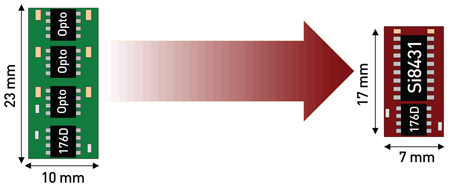
Illustrating the typical gains designers can achieve by switching from optical to RF isolation techniques, Figure 3 depicts the PCB area required to implement a Profibus interface. Profibus is an industrial serial communication standard that uses a twisted-pair serial link. It is similar to RS-485 or RS-422 and can operate in either a low-speed (1.5Mbps) or high-speed (12Mbps) mode. In this case the line interface chip is a 75ALS176D differential bus transceiver. To interface it to system logic with isolation requires three separate optocouplers (for receive, transmit and transmit-enable signals), as well as a number of passive components. The digital isolator package accommodates all three signal paths (with capacity to spare) and connects directly to system logic and to the ‘176D with no need for bias or other components.
While optocouplers have been the dominant signal isolation device for many years, the advent of the digital isolator gives designers a smaller, more integrated, faster and lower power alternative with none of the stability or wear-out mechanisms of optocouplers. www.silabs.com


