Digital power cuts time-to-market for industrial applications
Power designers have the possibility to tailor power solutions for specific functions
Given the range of industrial applications is extremely diversified ŌĆō from very small sensors powered by energy harvesting to mega processors used for process control and huge data computing capabilities required by some industrial equipment ŌĆō the challenge for power designers remains the selection of the most efficient power architecture across a large variety of applications.
Unlike the Information and Communication Technology (ICT) industry where boards often combine multiple processors and where the possibility of 3kW per board is moving closer, it is very common in industrial applications to design dedicated embedded computing functions for platforms such as MicroTCA or similar with dedicated boards for specific functions. The use of these cards makes upgrades or repairs easier for a site manager without needing to replace the entire system. The direct consequence of this type of architecture is that power designers have the possibility to tailor power solutions per board for specific functions, and to quickly implement new technologies such as dynamic energy management and control when upgrading systemsŌĆÖ controllers or data processing boards without having to wait for a complete system refresh.
Driving industrial applications
Industrial applications have used analog power modules for decades now, though with the growing demand for higher energy efficiency and tight control of energy, by 2008 the industrial segment had started to implement DC/DC converters and isolated POL (Point-of-Load) regulators with the PMBus. The first commercial application addressed the MicroTCA segment (see Figure 1), in which embedded digital PMBus-based DC/DC power modules simplified monitoring and control of the power unit. In addition, auxiliary boards started being populated with POLs with PMBus, initially being used for monitoring functions such as local temperature, output payload conditions and many other features, but rapidly system designers began to make use of the full performance benefits delivered by the PMBus.
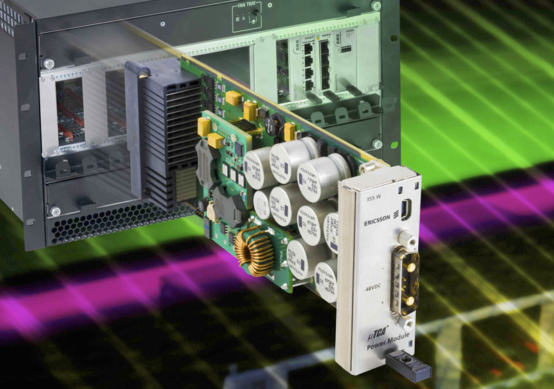
Click image to enlarge
Figure 1 ŌĆō MicroTCA power supply with digital DC/DC and PMBus interface
As happened in the ICT industry with the growing implementation of more complex ASICs, FPGAs and other processors, by 2012 industrial board power designers were also facing this situation and were having to design flexible power solutions that could meet specific profiles, not only during the design phase but also when the system was up and running.
For many designers used to a conventional power setup, designing a power solution based on relatively complex hardware combining analog, or analog-hybrid POLs and fixed components such as external clocks and multi-gate synchronization ICs (see Figure 2), they rapidly understood that the level of flexibility required in new applications made conventional processes significantly more complicated than that of simpler architectures.
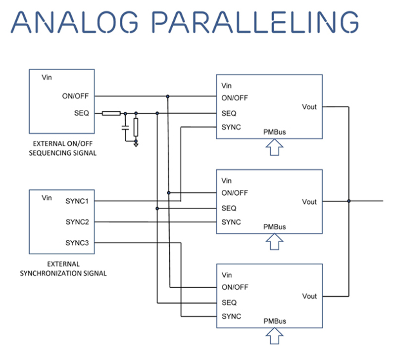
Click image to enlarge
Figure 2 ŌĆō External circuitry required for paralleling and phase spreading when using conventional analog or analog-hybrid POL
In addition, a power setup that required hardware modifications to adjust parameters such as sequencing or phase spreading would impact on time-to-market, which is crucial for many applications. It became a question of how best to make complex power architectures simple, efficient and reliable?
Simplicity in complexity
To achieve this required board power architects to explore different ways of working and consider new technologies such as digital power with built-in features. The most recent digital POLs (see Figure 3) with embedded features are making it possible to operate each module in a very complex power setup without adding external circuitry (Figure 4 shows the level of simplicity offered by digital power).
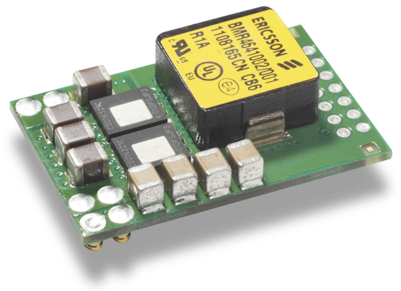
Click image to enlarge
Figure 3 ŌĆō Ericsson BMR464 40A digital POL with embedded and advanced features simplifying paralleling and phase spreading
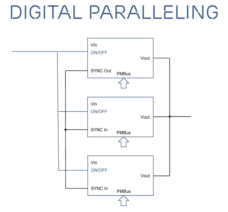
Click image to enlarge
Figure 4 ŌĆō Schematic for paralleling and phase spreading when using full digital POLs
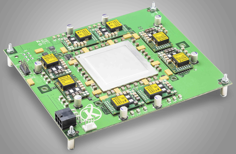
In industrial applications, embedded computing has gained in processing power, often using complex ASICs with multiple cores or quad-core multi-chip-module ICs. Considering that these types of applications require an average of 70A per channel, the embedded computing board could demand up to 300A when at operating at full computational performance. Figure 5 shows this type of application and ŌĆō despite the power setup requiring a number of features, which will be described later ŌĆō it is easy to see that very few components related to the power setup are actually required to efficiently power such a demanding application.
While it illustrates the simplicity of the hardware required, the highest benefits reside in the simplicity of the orchestration of different power sequences to optimize energy utilization and reduce ripple and noise, while also retaining a very high level of flexibility such as the ability to change any parameter and at any time without hardware changes.
Silence and flexibility in high current switching
At 300A, noise resulting from the switching stage could have a dramatic effect on performance. In conventional PCs, Voltage Regulator Modules (VRM) are built on multiphase topologies; but in the case of the application shown in Figure 5, while also enabling the lowest power losses and highest efficiency, each core needs to be powered by a dedicated pair of 40A modules connected in parallel. Phase spreading is implemented to reduce noise and via the use of interleaving, the four pairs of modules switch with the lowest level of ripple that is possible with this technology.
Click image to enlarge
Figure 5 ŌĆō Quad-core industrial embedded computing application requiring up to 300A (average 70A per core)
As mentioned previously, using conventional power architectures to implement paralleling with phase spreading requires significant hardware (as in Figure 2). However, it can be achieved using software such as the Ericsson Power Designer tool to visualize the phase-spreading effect on ripple and noise in real time.
The simplest way of phase spreading is allowing the products to operate individually from their own internally generated clock. This randomizes the occurrence of the edges of the switching frequency, which reduces the chances of high peak currents from the input source. However, this method also produces results that are not repeatable. A more controlled and effective way of phase spreading involves distributing the phase edges of each product in a group by operating them from a common switching clock. A single clock source can be used for all products and each product has its phase set to a different value throughout the cycle of the clock.
Phase offset and offset configuration
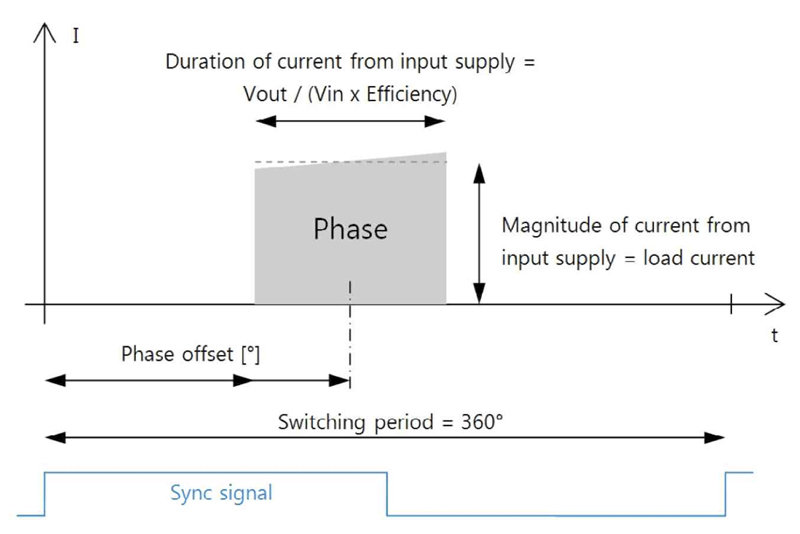
Assuming the POL regulator is supplied from a common input source, each converter is represented by a phase with a certain magnitude and duration in the switching period, as illustrated in Figure 6. The magnitude of the phase is the current drawn from the input supply, which approximately equals the output current of the rail. The duration of the phase as a fraction of the switching period equals the duty cycle of the rail, which in turn depends on the output voltage and actual efficiency of the converter. To achieve a phase spread, each phase needs an offset. The phase offset is defined as the time from the sync signal edge to the beginning of the phase duration.
Click image to enlarge
Figure 6 ŌĆō Phase shifting basic principles
For non-current-sharing rails, the phase offset is defined by the INTERLEAVE command by the Number In Group value (1-16) together with the Interleave Order value (0-15). The offset can be expressed in degrees or time according to the formula below, where TSW = 1/FSW is the switching period.
An example
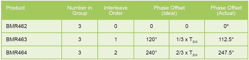
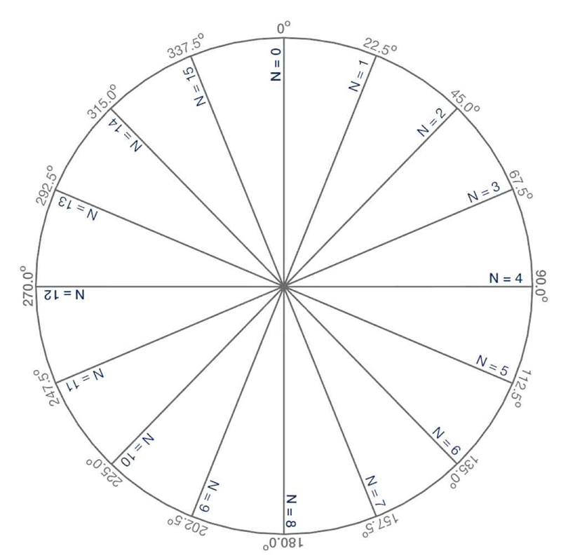
To demonstrate how simple it can be, consider a configuration based on three rails populated by 3E digital POLs delivering core and auxiliary voltages to a processor. Following the equations and using the values shown in Table 1, the ideal phase offsets can be calculated. By using the phase-offset resolution wheel (see Figure 7), these are the actual phase offsets to be entered into Ericsson Power Designer.
Click image to enlarge
Table 1 ŌĆō Example of the parameters used to calculate the offset
Click image to enlarge
Figure 7 ŌĆō Phase shifting, offset wheel
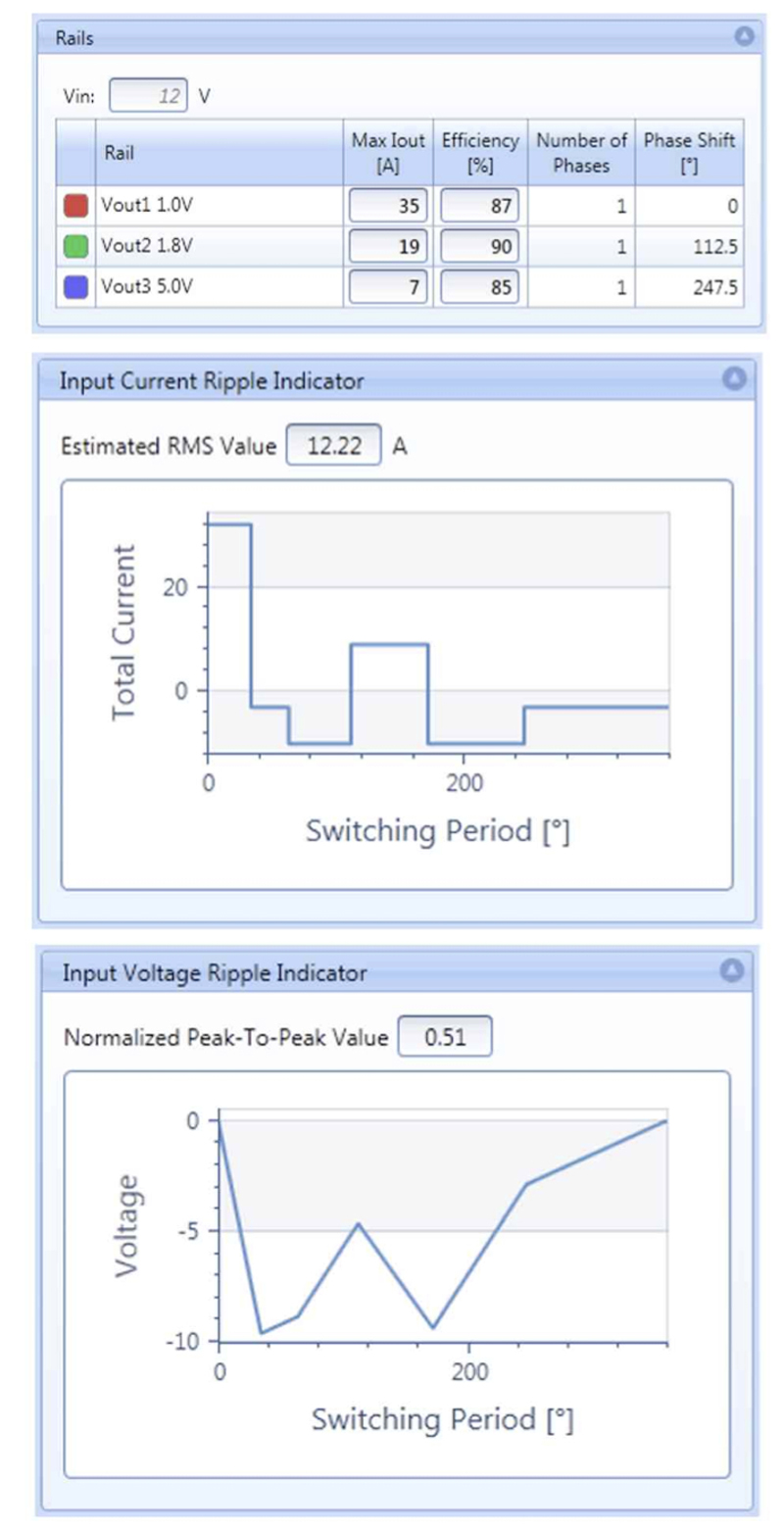
By default, the phase shift is set to zero with the result that all the rails will draw current at the same time, causing noise and uneven input current. To change this, phase spreading can be achieved by configuring specific phase offsets for each rail. The phase offset for each rail is indicated in the right-hand column of the table shown in Figure 8 and is also shown graphically by the position of colored block. To change the phase offset of a rail, power designers simply have to left-click and drag the corresponding colored block to the desired phase offset position. In this example, phase offsets are distributed equally across the period at 0┬░, 112.5┬░ and 247.5┬░.

Click image to enlarge
Figure 8 ŌĆō Ericsson Power designer screenshot of phase spreading interface
Another interesting possibility offered by digital power and simulation tools is the visualization of input current and voltage ripple with the optimization of phase spreading (see Figure 9), making it possible to reduce the amount of filtering.
Click image to enlarge
Figure 9 ŌĆō Ericsson Power Designer phase spreading and input current and input voltage ripple indicators
The Input Current Ripple Indicator provides an estimated RMS value of the total input current ripple of the rails, as well as a graph showing the variation of the total input current along the switching period. The target is a minimized RMS value, which means a ŌĆśsmoothedŌĆÖ out input current. The Input Voltage Ripple Indicator provides a normalized peak-to-peak value of the total input voltage ripple of the rails, in addition to a graph showing the variation of the input voltage along the switching period. The normalized peak-to-peak value will be 1 in the case where all phases have zero phase offset. As offsets are introduced the peak-to-peak value will be reduced. The target is a minimized peak-to-peak value.
Optimizing phase spreading
Power designers have two possibilities: manual or automated optimization. In the case of a simple system without current-sharing rails, most of power designers will likely use the manual optimization, which follows the previously described sequence (left click and drag phases to the desired offsets) and visualize the result with the adjustment.
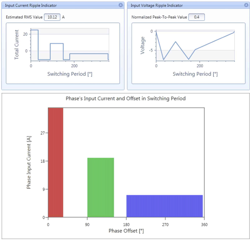
For more complex systems with current-sharing rails or a larger amount of rails, finding the optimized phase offsets manually may not be an easy task. With a single click on the ŌĆśOptimizeŌĆÖ button, Ericsson Power Designer will automatically find an optimized configuration of phase offsets. Trying this on the example, a spread can be achieved with the same input current RMS value as in the manual optimization, but with a lower peak-to-peak input voltage ripple (see Figure 10). The increased offset difference between the higher current 1.0V and 1.8V rails affects the input voltage waveform, so that the normalized peak-to-peak value is reduced from 0.5 to 0.4.
Click image to enlarge
Figure 10 - Automatic phase spreading representation
Saving time-to-market
The example presented above clearly demonstrates the benefits that can be delivered by digital power when implemented in industrial applications, such as simplified design and shorter time-to-market. What is more, in demanding applications such as that shown in Figure 5, employing know-how and expertise in the field and implementing digital power at its best can result in a five-fold reduction in time-to-market.