A properly designed digital power management system can facilitate smart energy decisions
System architects of embedded systems, networking, and datacom equipment are constantly being pushed to increase the data throughput and performance of their systems as well as add functionality and features. At the same time, pressure is being applied to decrease the system’s overall power consumption. For example, in data centers, the challenge is to reduce overall power consumption by rescheduling the workflow and moving jobs to underutilized servers, thereby enabling shutdown of other servers. However, in order to meet these demands, it is essential to know the power consumption of the end-user equipment. To achieve this aim, a properly designed digital power management system can provide the user with power consumption data, facilitating smart energy management decisions.
To better understand this concept, consider if you will, the real life example of an embedded system. Most embedded systems are powered via a 48V backplane. This voltage is normally stepped down to a lower intermediate bus voltage, typically 12V, and then further stepped-down to 3.3V to power the racks of boards within the system. However, most of the sub-circuits or ICs on these boards are required to operate at voltages ranging from sub 1V to 3V at currents ranging from tens of milliamps to hundreds of amps. As a result, point-of-load (PoL) DC/DC converters are necessary to step-down from this intermediate bus voltage to the desired voltage required by the sub-circuits or ICs. And, to further complicate matters, these rails have strict requirements for sequencing, voltage accuracy, margining and supervision.
Since there can be upwards of 50 PoL voltage rails in a datacom, telecom, or storage system, system architects need a simple way to manage these rails with regards to their output voltage, sequencing and maximum allowable current. Certain processors demand that their input/output (I/O) voltages rise before their core voltage, alternatively certain DSPs require their core voltage rise before their I/O. To further complicate matters, power-down sequencing is also necessary. Consequently, designers need an easy way to make changes to optimize system performance and to store a specific configuration for each DC/DC converter in order to simplify the overall design effort.
Safety is key
Moreover, in order to protect expensive ASICs from the possibility of an overvoltage condition, high-speed comparators must monitor the voltage levels of each rail and take immediate protective action if a rail goes out of its specified safe operating limits. In a digital power system, the host can be notified when a fault occurs via the PMBus alert line and dependent rails can be shut down to protect the powered devices such as an ASIC. Achieving this level of protection requires reasonable accuracy and response times on the order of tens of microseconds.
For these reasons, digital power conversion ICs need to provide highly accurate digital power system management with their high resolution programmability and fast telemetry read-back for real-time control and monitoring of critical point-of-load converter functions. They must deliver high efficiency synchronous step-down conversion with I2C-based PMBus interface with over 100 commands and have onboard EEPROM. These devices must combine best-in-class analog switching regulator controllers with precision mixed signal data conversion for unsurpassed ease of power system design and management. Finally, it is also imperative that they be supported by the software development systems with easy-to-use graphical user interfaces (GUIs).
Smaller is faster
Analog power advances are usually the result of circuit concepts that are developed. Very few of these cross manufacturer boundaries and rarely end up used by multiple companies in multiple products. This is unlike digital advances in process, which tend to be proliferated across the industry. Analog IC design concepts that have proliferated over time include chopper-stabilized amplifiers, delta sigma A/D converters, BurstMode voltage regulators, band-gap references, and 3-terminal regulators. However, the accumulated knowledge of making complex functions in different processes continues to advance. This accumulated knowledge allows still higher functionality mixed signal ICs to be generated each year.
The continuing push for smaller line widths in digital ICs has had its effect on analog as well. These processes continually get faster and enhance the speed of analog ICs made on these processes. Analog to digital (A/D) converters are a good example of where smaller line widths have led to faster A/D converters. Circuit advances improve the resolution as well as the speed, and new devices convert at 200 megabits per second with 16 bits of resolution. There’s no reason to think that they will not continue to accelerate in speed and precision as techniques are developed to go faster and be more accurate.
These smaller line widths make practical some digital functions that were previously impractical in analog ICs. Power supply controllers with digital read back of voltage, current and status are achieved on the same chip as the power functions. A side benefit to these smaller line widths is the inclusion of DMOS transistors on the small feature digital process. These DMOS devices can handle high voltage as well as high current and allow the complete integration of power converters, switching regulators with both power and control on the same device.
Circuit advances in bipolar technology yield incrementally better references, amplifiers, and RF ICs. These enhancements are due to refinement in the circuitry and optimization rather than any type of breakthrough due to process. The competitive landscape for analog ICs keeps all manufacturers on their toes in trying to improve their products. However, it should be noted that since analog IC performance is based on real world parameters, the ICs can end up at the theoretical limits of performance. Once the theoretical limitation is approached, further improvements are just not possible. That’s why some of today’s best-selling and most widely used ICs were designed over 20 years ago and have not changed in the interim.
Digital Power System Management (DPSM)
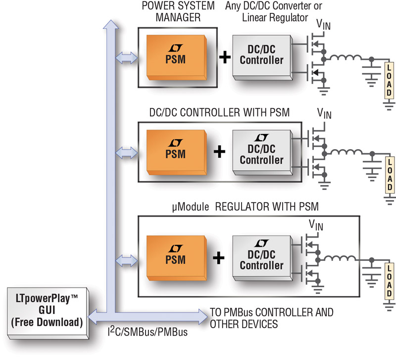
With this background, what does the system architect have to do in order to configure a digital power system management solution for their end product? One of the primary objectives will be to design a system so that it can be easily configured and monitored via a digital communications bus. This will be achieved by utilizing one of the following; I2C, SMBus or PMBus. Either of these buses can enable on-demand telemetry capability to set, monitor, change and log power parameters of any PoL converter configuration within the system. A simplified snapshot of such a system is shown in Figure 1.
Click image to enlarge
Figure 1. Typical Digital Power System Management System Configuration
As can be seen in this example, the PoL converters illustrate 3 different topology configurations. At the top of the figure, a power system manager chip is used alongside a conventional DC/DC converter. The DC/DC converter can be of any topology and have any degree of integration since it is the power system manager that will allow it to be interfaced, controlled and monitored via the communication bus. The middle PoL converter demonstrates an increased level of integration, namely, that the DC/DC converter has the power system management built-in (in the same package). And finally, the bottom PoL converter is a compact module which incorporates the power system manager, the DC/DC converter and all its associated external components into a single form factor (Linear calls these a µModule® regulator).
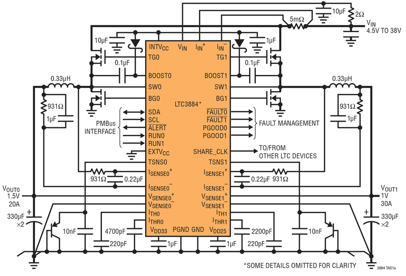
Linear Technology offers a broad selection of devices to allow systems designers a choice of how to configure their digital power system requirements from system managers and their associated PoL DC/DC converters, so a single digital power µModule regulator. Figure 2 shows the schematic of the LTC3884, a dual output PolyPhase step-down controller for ultralow DCR sensing with digital system power management.
Click image to enlarge
Figure 2. LTC3884 schematic delivering 1.5V at 20A & 1.0V at 30A
The LTC3884 provides two high-current outputs from a wide 4.5 to 38V input voltage range with an I2C-based PMBus compliant serial interface. The controller employs a constant-frequency current-mode architecture, together with a novel scheme which enhances the signal-to-noise ratio of the current sense signal to provide excellent performance in ultralow DCR applications. Programmable loop compensation allows the controller to be compensated digitally. Switching frequency, channel phasing output voltage, and device address can be programmed both by the digital interface as well as external configuration resistors. Additionally, parameters can be set via the digital interface or stored in EEPROM. Both outputs have independent power good indicators and fault functions. Finally it is supported by Linear’s LTpowerPlay software development tool with GUI (more on this later).
There may be applications where a higher level of integration in the PoL converter is desired, especially in applications where the output currents are not so high, such as in the 4 to 6A range. It is for these circumstances that Linear developed the LTC3815, a 6A monolithic synchronous step-down converter with digital system power management (see Figure 3). This PoL converter uses a phase lockable controlled on-time constant frequency, current mode architecture to provide extremely fast transient response and allows operation at the very low on-time required to regulate low output voltages at high switching frequencies. The output voltage is programmable from 0.4V to 75% of the input voltage with a single external resistor or with an external voltage reference through the reference input pin. The output can be margined up or down 25% in a little as 0.1% increments with a standard PMBus interface.

Click image to enlarge
Figure 3. LTC3815 Application Schematic for 2.2V to 5V Input down to 0.4V at 6A
The LTC3815’s operating frequency is programmable form 400kHz to 4MHz with an external resistor or for switching noise sensitive applications or it can be synchronized to an external clock over the same range. Finally, its serial interface can also be used to read back fault status and both time-averaged (~4ms) and peak input/output current, input/output voltage and temperature.
LTpowerPlay universal GUI for DPSM products
A key advantage of a system architected with DPSM products is that with the right GUI it is easy to communicate with each individual PoL converter within in the system. So, from the onset, Linear decided to develop a GUI that was a complete development platform which could be easily used with all of the different types of products it offered in its DPSM product portfolio – the LTpowerPlay windows-based development environment. Not only does this software make it easy to control and monitor multiple Linear PMBus-enabled devices simultaneously, it also allows modification of the DC/DC converters configurations in real time be downloading system parameters to the internal EEPROM of the individual devices (see Figure 4).
Click image to enlarge
Figure 4: The LTpowerPlay windows-based development environment makes it easy to control and monitor multiple Linear PMBus-enabled devices simultaneously
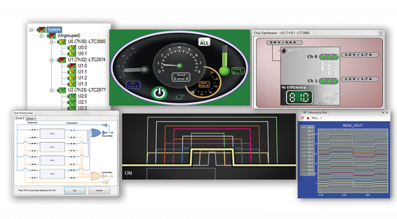
This reduces design development time by allowing system configurations to be adjusted in software rather than resorting to the time honored tradition of swapping out components and rewiring boards with a solder iron! But it doesn’t stop there, once an end system has been deployed in the field, such as a data center, then the system can be adjusted real time by an overseer by simple updating operation parameters of the PoL converters via an applicable interface using this GUI. Figure 5 shows a typical screen shot of Linear’s LTpowerPlay dashboard that a user would see when interrogating their system.
Click image to enlarge
Figure 5. A Snapshot of a Typical Dashboard Screen Shot of the LTpowerPlay GUI
All Linear PMBus products are supported by this software development system which can help designers quickly debug systems both during initial development and then when they are installed at a user’s site. It quickly and easily allows monitoring, control and adjustment of supply voltages, limits and sequencing. Furthermore, production margin testing is easily performed using a couple of standard PMBus commands.
Looking forward
Having digital power management capability in datacom, telecom or storage systems provides the system architects with the necessary tools to develop “green” power systems that meet target performance (compute rates, data rates and etcetera) with minimum energy usage at the point of load, board, rack and even installation levels. This reduces infrastructure costs, as well as the total cost of ownership over the life of the product. And while it might take the fun out or the traditional solder iron and rewiring approach to debugging hardware systems, the software programmability of DPSM significantly reduces the debug time normally associated with such endeavors.