Author:
Jonathan Dodge, P.E., UnitedSiC (now Qorvo)
Date
05/02/2022
 PDF
PDF
Click image to enlarge
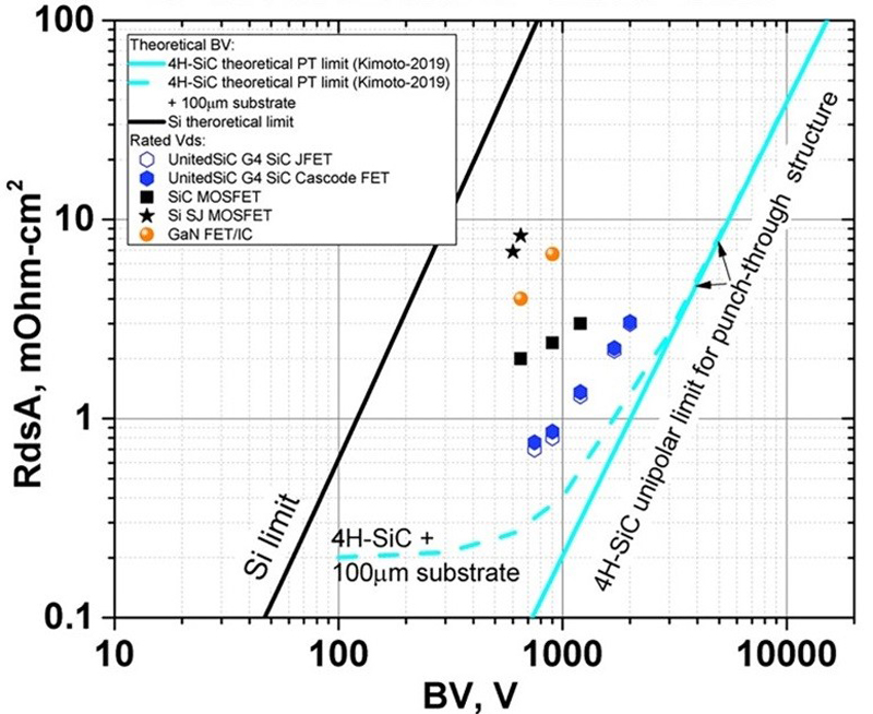
Figure 1: Unipolar RDS∙A versus breakdown voltage data by technology (room temperature)
The silicon carbide (SiC) JFET is arguably the most ideal switch technology for an application requiring minimum conduction loss, such as solid-state relay (SSR), solid-state circuit breaker (SSCB), and high power motor drive. Its low on-resistance per unit area (RDS∙A) and fast switching compete well with mechanical relays and IGBTs. The SiC JFET is also very rugged, with repetitive avalanche and short-circuit capabilities and no parameter drift. This article highlights two additional features: a way to further reduce conduction loss by 15+%, and a means of real-time, on-chip temperature sensing. The normally-on SiC JFET is made normally-off with an enable MOSFET plus a couple Zener diodes. In this article, a brief outline of SiC JFET characteristics is followed by a design example that shows how to utilize the SiC JFET capabilities.
SiC JFET Characteristics
1.1 Conduction Loss
All device types benefit from wide bandgap technology such as gallium nitride (GaN) and silicon carbide (SiC). However, the SiC JFET has far superior RDS∙A due to the high breakdown voltage (BV) of SiC combined with the elimination of the MOS channel. The result is a device that comes much closer to the theoretical unipolar RDS∙A-BV limit of the material, as shown in Figure 1.
The Gen4 SiC JFET RDS∙A-BV technology curve is closest to the theoretical material limit, followed immediately by the Gen4 SiC JFET cascode (to be discussed). Following further behind are the SiC MOSFET, GaN FET, and finally the silicon-based super-junction (SJ) MOSFET. It is this RDS∙A-BV advantage that enables the cost-effective manufacture of 1200 V rated JFETs with RDS(on) well under 10 mΩ at room temperature, without compromising the reverse-bias safe operating area (RBSOA) or other key parameters. Such low on-resistance combined with fast switching speed and very wide RBSOA make the SiC JFET a compelling replacement for mechanical relays and circuit breakers.
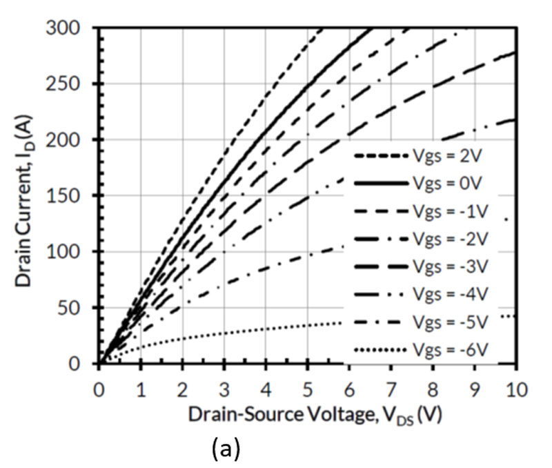
There is some very low hanging fruit to be harvested with direct drive of a SiC JFET. First is a further reduction in on-resistance by forward-biasing the gate, as evident in the output characteristic of a 1200 V, 7.6 mΩ Gen3 JFET, shown in Figure 2(a).
Click image to enlarge
Figure 2a: Output characteristic of UJ3N120008 at 175 °C
Click image to enlarge
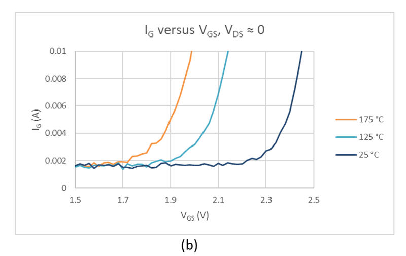
Figure 2b: Gate current versus gate-source voltage of UJ3N12035K3S
Driving the SiC JFET gate positive by 2 V results in a 16% reduction in on-resistance, at 175 °C, and even more reduction at lower temperatures. The reason for this is a further enhancement of the JFET channel. Injection of minority carriers in the gate-source P-N junction is at a very low level and has negligible effect on conduction loss or switching.
Figure 2(b) curve tracer data shows gate current versus gate-source voltage at various temperatures of a smaller 1200 V, 35 mΩ Gen3 JFET. The gate-source P-N junction has a very linear forward voltage versus temperature at a given gate current, which for Gen3 SiC JFETs is -3.22 mV/°C. The gate current should be high enough to be above the noise floor, which from Figure 2(b) is about 2 mA. Gate current in the range of 5 to 20 mA is recommended. The SiC JFET gate can handle Amps of forward bias current without damage, so current in the range of milliamps is certainly safe.
1.2 Reliability and Durability
Elimination of a MOS channel eliminates mechanisms for parameter drift in the SiC JFET, even after short-duration, high temperature events, including avalanche, short-circuit, and surge current of either polarity. Of critical importance for relay and circuit breaker applications is the peak current that can be safely and repeatedly switched off. A demonstration of this is shown in Figure 3.
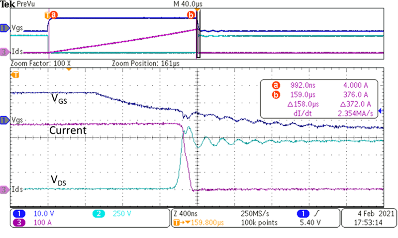
Click image to enlarge
Figure 3: Turn-off of UF3SC120009K4S at 376 A, 680 V
After a somewhat slow ramp up, a SiC JFET cascode quickly switches off a 376 A inductive load with a 680 V DC link. This 8.6 mΩ cascode can safely and repeatedly switch off up to 550 A with unchanged parameters provided overheating is avoided. Current can be of either polarity, or in other words, flowing in forward or reverse direction. The low conduction loss is needed for normal operation, while the high turn-off current is mandatory for emergency shutdowns. An important advantage over mechanical switches is the lack wear, so the number of switching events is in the range of millions as opposed to hundreds to thousands as with mechanical switches.
1.3 Switching Speed
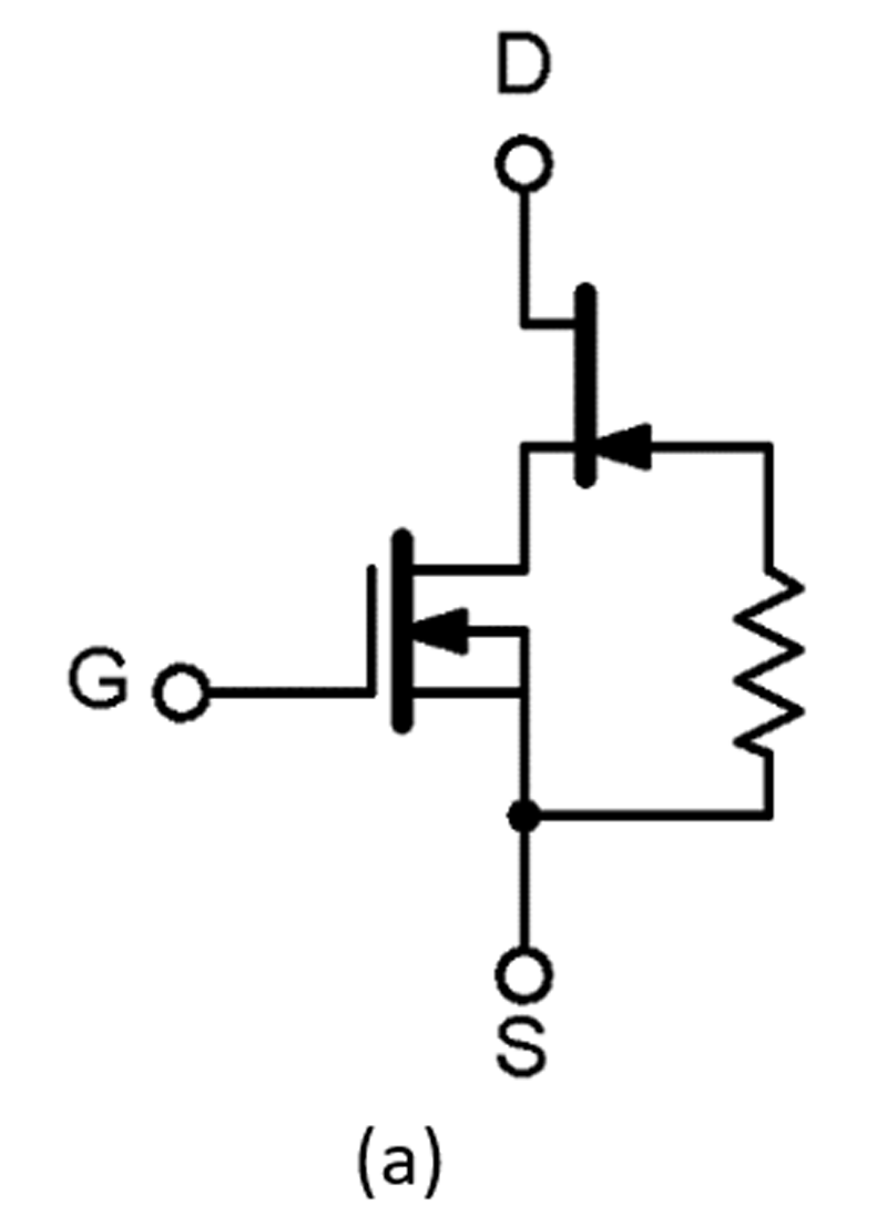
As with any device type, the switching speed of a JFET depends much on the circuit. Due to its normally-on characteristic, the SiC JFET is often co-packaged with a low-voltage silicon MOSFET in the normally-off cascode configuration, as shown in Figure 4(a).
Click image to enlarge
Figure 4a: SiC JFET connected in series with a low-voltage silicon MOSFET to form a normally-off cascode
Click image to enlarge
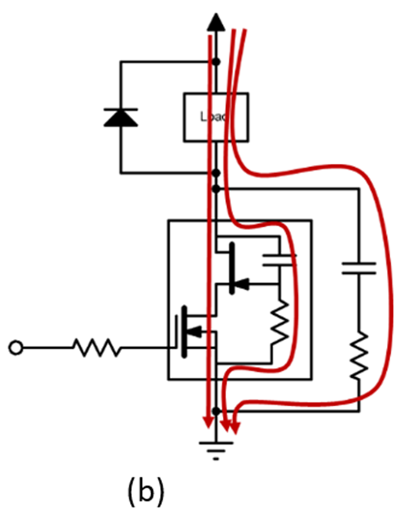
Figure 4b: Cascode switching off inductive load with RC snubber
Click image to enlarge
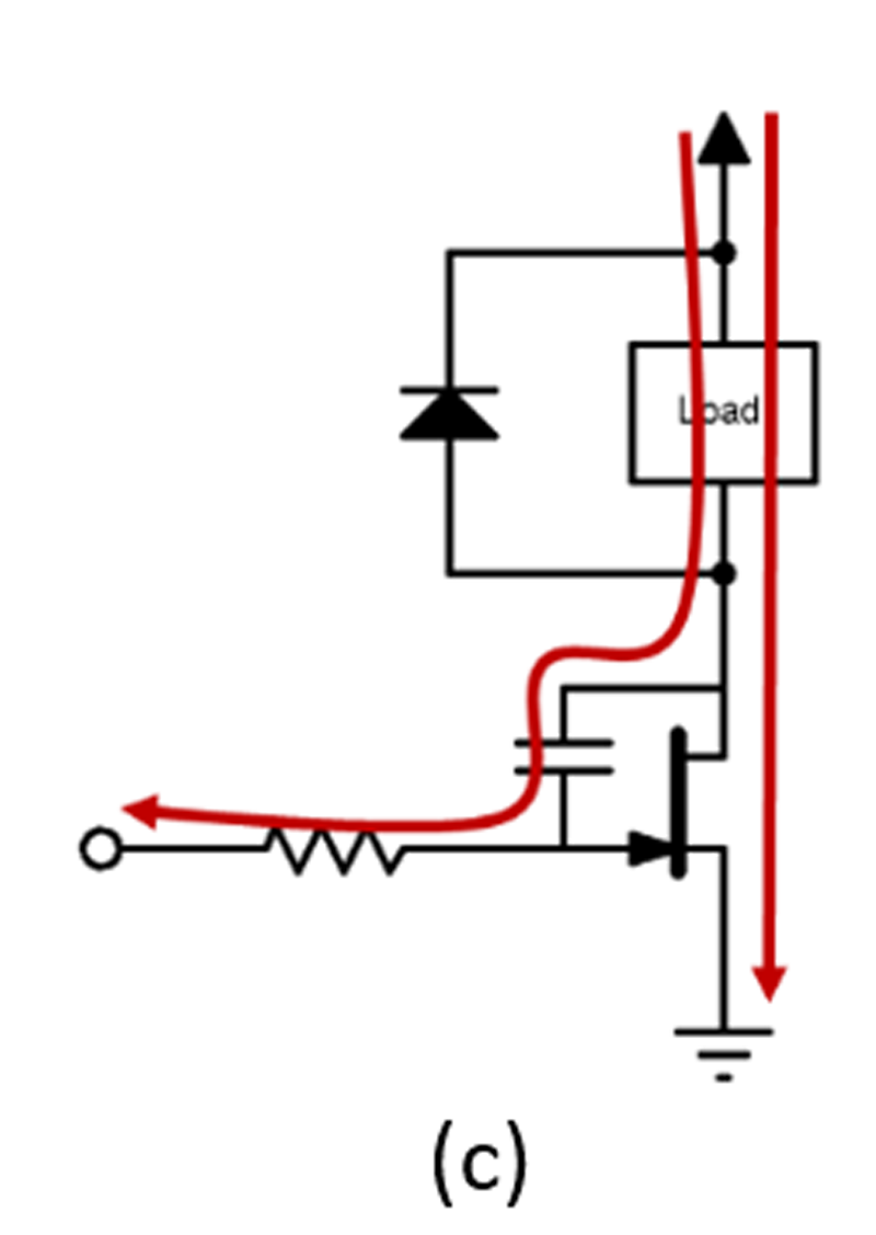
Figure 4c: JFET switching off inductive load
The SiC JFET has practically no drain-source capacitance (no P-N junction in the current path). In the cascode configuration with the shunted JFET gate, this means that the cascode has practically no drain-gate capacitance. Viewing Figure 4(b) during cascode turn-off, the voltage slew rate is mostly determined by the load current and drain-source capacitance. The current through the JFET gate-drain capacitance flows through the internal JFET gate resistance instead of through the external MOSFET gate resistance. This JFET gate resistance is fixed, and hence the reliance on external snubbers for switching speed control. Much of the effort involved with utilizing the cascode is focused on slowing the switching speed rather than speeding it up.
The SiC JFET itself has substantial gate-drain capacitance as well as gate-source capacitance, and with no drain-source capacitance, the drain-gate capacitance is charged/discharged through the gate impedance, as shown in Figure 4(c). This means that the turn-on and turn-off slew rates can be controlled by the gate impedance without relying on snubbers. This is another motivation for direct drive of the SiC JFET. Gate charge is higher but a good tradeoff, especially SSR and SSCB considering the drive power required for mechanical relays.
Both the cascode and the direct-drive JFET can switch an inductive load in tens of nanoseconds, even at very high current levels. Mechanical relays on the other hand typically switch in the milliseconds range, orders of magnitude slower. This means that arc flash events are eliminated with the solid-state switch, which has huge implications for system safety.
2 Direct Drive Design Example
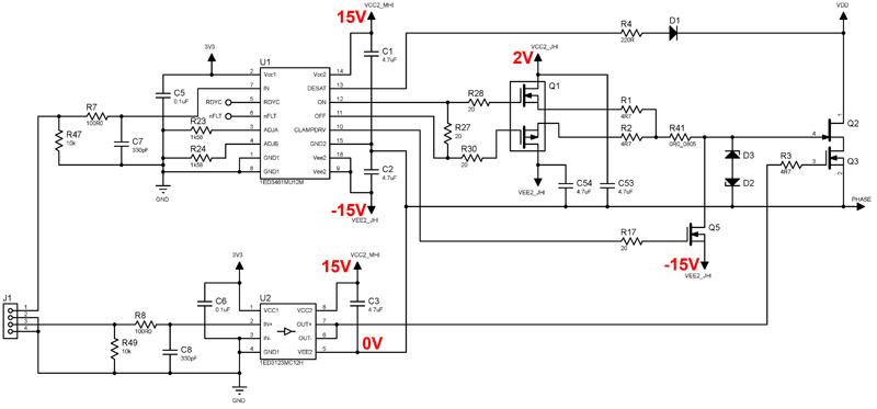
This example circuit is the high-side portion of a half-bridge circuit using off-the-shelf gate drivers and components to implement positive voltage overdrive and DESAT detection. Two gate drivers drive the SiC JFET and the 1 mΩ, 30 V silicon MOSFET separately, as indicated in the schematic of Figure 5. The MOSFET is used as an enable, meaning it is turned on at system power-up and left on. This SiC JFET + MOSFET combination has a typical RDS(on) of 8.8 mΩ (SiC JFET + MOSFET) at room temperature. The JFET gate driver U1, part number 1ED3461MU12MXUMA1 from Infineon, drives the JFET and has DESAT and external Miller clamp features. The MOSFET driver U2, Infineon part number 1ED3123MC12H, is simpler, but like the JFET driver has built-in galvanic isolation and can work with ±15 V supplies.
The first requirement to drive the JFET is to switch on with about +2 V and off with around -15 V. Existing gate drivers have undervoltage lockout (UVLO) set for different voltage ranges, such as +15/-5 V. To make the gate driver work, a buffer MOSFET is used as a voltage level reducer. This is the upper, N-channel MOSFET of Q1 in Figure 5.
Click image to enlarge
Figure 5: Schematic of a high-side direct drive SiC JFET copackaged with enable MOSFET
A voltage regulator (not shown) supplies the 2 V to the drain of the N-channel buffer MOSFET, whereas the gate of this MOSFET is driven to ±15 V. This N-channel MOSFET in turn drives the JFET gate to +2 V when on. The JFET is driven off to -15 V through a P-channel buffer MOSFET in the Q1 package. This lower buffer is optional because the gate driver U1 has separate outputs for turn-off and turn-off, and it could directly drive the JFET gate to -15 V.
The 18 V Zener diode D2, as oriented in Figure 5, makes the SiC JFET + MOSFET function as a cascode if gate drive power is off, making them together normally-off even if the DC link is energized. This Zener diode therefore prevents shoot-through if control power is unexpectedly lost. D3 allows the JFET gate to be forward-biased.
Control of the JFET switching speed is by adjusting the values of the turn-on and turn-off gate resistors R1 and R2, respectively. R41 is a zero-Ohm jumper test point. DESAT functions as with an IGBT or SiC MOSFET. The Miller clamp is implemented with an external MOSFET Q5, but a gate driver with an internal clamp would also work fine. The clamp helps to keep the JFET off during high dV/dt transients, as with IGBTs or SiC MOSFETs.
The temperature of the JFET can be measured if the source of the JFET is available outside the package. This can be done by measuring the voltage across R1 and across the JFET gate-to-source. This indicates the gate current, which combined with the gate-source voltage can be used to lookup the JFET chip temperature. This is a real-time, on-chip, low delay temperature measurement with multiple uses.
Another way to sense temperature is using the leakage current of the electrostatic discharge (ESD) protection diodes that are built into the MOSFET gate. Being a diode, they have a linear VF versus temperature characteristic that makes MOSFET chip temperature sensing very straightforward simply by knowing its bias voltage. Since the MOSFET remains on during operation, it is free from switching events that must be blocked by a diode and blanked out until the signal settles; the MOSFET gate leakage current is constant because the MOSFET gate-source voltage is constant. Furthermore, if the MOSFET chip is attached to the top of the JFET chip, its temperature is slightly higher than that of the JFET chip because the MOSFET has no switching loss and its on-resistance is a fraction of the JFET on-resistance.
With minimal additional cost and off-the-shelf components, this direct drive circuit reduces the on-resistance from the SiC JFET by more than 16%. The enable MOSFET adds some, but not all of that back, and the SiC JFET switching speed is directly controlled. Finally, DESAT and Miller clamp features enhance the reliability of circuit.