Drive Your Power Applications to the Next Level with GaN
GaN HEMTs full potential realized with dedicated GaN gate driver
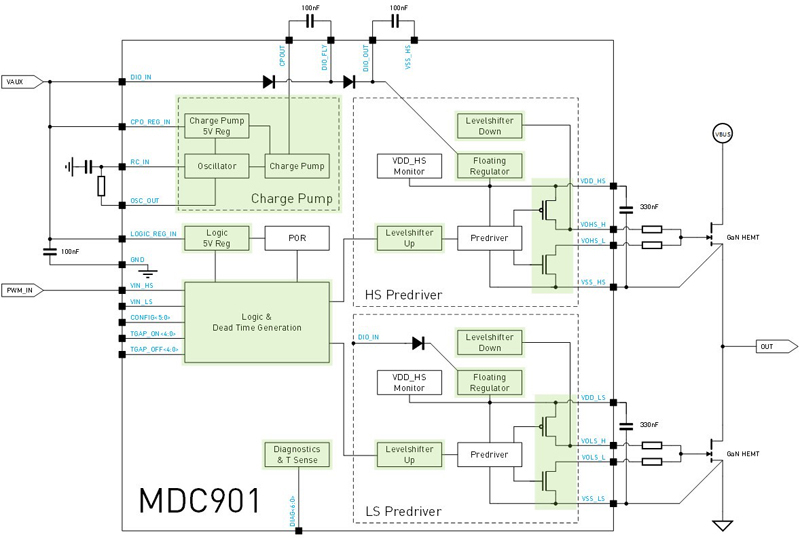
Figure 1: The block diagram of the MDC901 GaN gate driver
The entire ecosystem surrounding GaN HEMTs, which includes active and passive components like gate drivers, inductors and capacitors as well as the design techniques to implement the devices effectively, must quickly evolve to realize GaN’s full potential. As the device directly controlling the GaN HEMTs, the gate driver plays the most critical role in the performance and reliability of the GaN devices. This requires optimizing the gate-drive. The gate-source voltage must be tightly controlled in terms of both voltage and time. In a typical half-bridge, the high-side gate-source voltages are floating up and down at high voltage (e.g. 200V) and at high dV/dt (e.g. 100V/ns). Such stringent operating conditions require optimized and dedicated gate driver technology. Getting the maximal benefit from a GaN stage requires careful driving, avoiding the pitfalls along the road.
To tackle these hurdles, MinDCet introduced the MDC901 GaN gate driver. The depicted block diagram in Figure 1 provides an overview of the key functionality, solving the major pitfalls when driving GaN devices.
High Slew Rates
The high electron mobility of GaN presents a significant benefit in the power stages, their fast switching ability. The fast switching equates to high slew rates, potentially leading to very low switching losses. The quick switchover between low and high-side transistors causes the load current to alternate very quickly, putting constraints on the bus voltage decoupling and its parasitic bus loop inductance.
The MDC901 has separate pull-up and pull-down paths, to allow for tuning of the slew-rate of the output stage, while maintaining a low impedance pulldown path for the GaN transistor to avoid parasitic turn-on.
Deadtime Control
The deadtime in a half-bridge is the time between the turn-off event of one transistor and the turn-on event of the complementary bridge transistor. For optimal efficiency, the deadtime needs to be tuned for a given application.
The MDC901 has separate deadtime control for turn-on and turn-off can through a series of digital inputs. This allows tuning of the deadtime for a given application, either static or dynamically. Additionally, a fail-safe operation mode is present, which sets the deadtime based on sensing the GaN gate voltage.
Gate Overcharging
In non-isolated gate-drive applications, the gate driver is supplied through bootstrapping of the low voltage supply. This technique will charge the high-side gate driver supply decoupling capacitor through a fast high-voltage diode. Inductive voltage spikes or non-zero deadtime will cause negative half bridge output voltages, which could lead to detrimental overcharging for the GaN gate.
The MDC901 avoids the risk of gate-overcharging during negative voltage operation by placing fully floating regulators both in the high-side and low-side domain after the bootstrap diode. This results in a well-defined and robustly protected gate driver voltage.
Negative Output Voltage Operation
The negative swing of the output driver voltage depends on the parasitic source inductance and the load conditions of the power converter, which can be poorly predicted. For predictable operation, a guarantee that the converter bridge can always be controlled is required, even when entering negative voltage relative to the supply grounds.
The MDC901 allows for guaranteed negative output voltage operation down to -11V, allowing accurate gate control even under high inductive currents. This has been accommodated by a specifically designed level shifter and floating supply generation.
High duty cycle operation
Bootstrapped operation of a gate driver is a simple and effective means to provide charge to control the high-side transistor, for example, in a half-bridge. Unavoidably, the bias for supporting circuitry needed in the predriver system - which causes the bootstrap voltage to leak away, sets a maximum on the duty cycle that can be maintained or limits the modulation depth that can be used.
For high duty cycle applications (e.g. motor drivers and class-D amplifiers), it is mandatory to maintain a high-side on-state for longer periods of time. This functionality was implemented in the MDC901 by an integrated charge pump, compensating for DC bias under 100% duty cycle conditions.
The MDC901 provides a high-end and feature-rich solution to driving GaN transistors in a reliable way for maximizing performance in the given application with a clean and fast switching node voltage. The driver was developed for DC-DC solutions, but can be used for all other GaN driving applications like audio class-D, motor drivers, and electronic fuse applications requiring true 200V capability.
User Experience of the MDC901 Evaluation Board (EVB)
A dedicated evaluation board (MDC901-15I-EVBHB) allows the user to experience the full capabilities of the gate driver. The EVB is a flexible step-down converter platform, consisting of a buck topology built around the MinDCet MDC901 gate driver, controlling the 150V Innoscience INN150LA070A HEMT half-bridge and a WE-HCF 1.4uH/31.5A power inductor. Evaluation kit implementations using different GaN technologies and topologies are under development and available upon request.
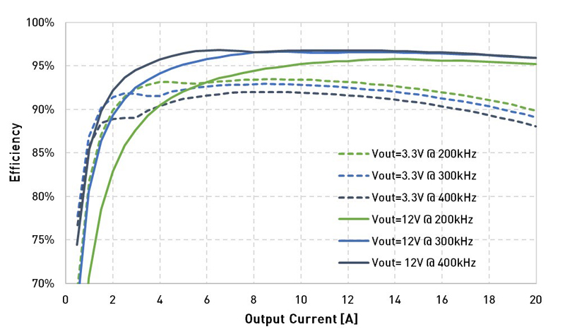
The power of GaN can be demonstrated with a high input/output ratio buck converter. As an example, we have measured a 48V to 3.3V use-case, using the EVB. The low duty cycle (ca. 6.8%) benefits from the fast switching transient speeds, resulting in a 10 to 15 percent efficiency increase over an equivalent MOSFET-based converter at the same switching frequency. The efficiency measurement in Figure 2 exemplifies that despite GaN’s capabilities, the conversion efficiency decreases as switching frequency increases. Already at moderate switching frequencies of 200 kHz, a decrease of nearly 1 percent efficiency per additional 100 kHz in switching frequency can be observed over the measured frequencies from 200 to 400 kHz. This contradicts the high-frequency GaN paradigm and indicates that the higher efficiencies possible with GaN is not necessarily achieved at higher frequencies. Although, this may depend on the actual voltages and their ratio. Looking at the 12V output case, the efficiency is not notably affected in this frequency range at moderate to high output loads. In fact, the efficiency benefits from the higher switching frequency at low loads due to the reduced ripple current in the inductor, which in-turn reduces the inductor AC-losses and lowers conductivelosses in the GaN HEMTs.
Click image to enlarge
Figure 2: The measured efficiency as a function of the output current for a 48V to 3.3V and 48V to 12V GaN-based buck converter, at different switching frequencies
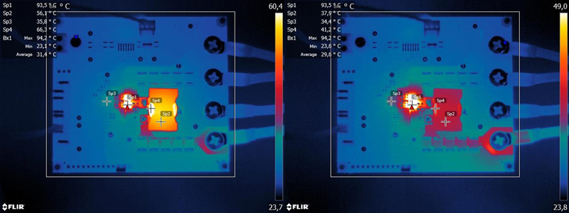
Even with the high efficiency of GaN, the DC-DC converter still requires proper thermal management to dissipate the losses. As the GaN HEMTs are bottom cooled, a pushpin, forced-air heat sink is installed on the EVB backside. Depending on the operating conditions (such as ambient temperature and power level), the fan can be switched on. Thermal images, taken at thermal steady state, are shown in Figure 3. Set points of 48V bus and 12V and 3.3V out, both at 16A output current and a switching frequency of 300kHz. For 3.3V out, the resultant efficiency is 91.3% with a total power dissipation of 5.0W. At 12V out, the efficiency is 96.4% with a power dissipation of 7.2W. In the low duty cycle case of 3.3V out, the main power loss occurs in the GaN power stage, where the inductor experiences significant losses in the 12V case. The limited temperature rise in the MDC901 is primarily due to conduction from the GaN HEMTs. This clearly demonstrates that depending on the use case the power dissipation distribution may shift between inductor and GaN HEMTs. Moreover, it shows for the 3.3V case that the driver needs to be able to cope with increased operating temperatures since it is in close proximity of the GaN.
Click image to enlarge
Figure 3: The thermal images of the MDC901-15I-EVBHB for 48 V to 12V (left) and 3.3V (right) GaN-based buck converter use cases with an output current of 16A