Large-area high-power GaN transistors with on-chip drivers can be easily driven
High voltage normally-off GaN transistors are being introduced into the marketplace, and most of these devices will have low threshold voltages of below 2.5 Volts. This presents a severe challenge to conventional drivers, particularly when these very large GaN devices are used to provide 100 - 400A of switching current, as is typical in automotive motor drive circuits.
Conventional drivers can be used if they are carefully mounted in very close proximity to the GaN power switch. Thermal issues then become the dominant concern because of the driver’s self-heating when combined with the heat generated by the GaN power switch.
The input capacitance of GaN power switches increases significantly and non-linearly at low drain voltages. The gate of the GaN transistor must therefore be cleanly clamped to a well-positioned source sense connection. The switching transition losses increase substantially if the gate - source voltage is not cleanly brought well below the GaN device’s threshold voltage or rapidly raised to the maximum allowed gate voltage.
Using an on-chip driver
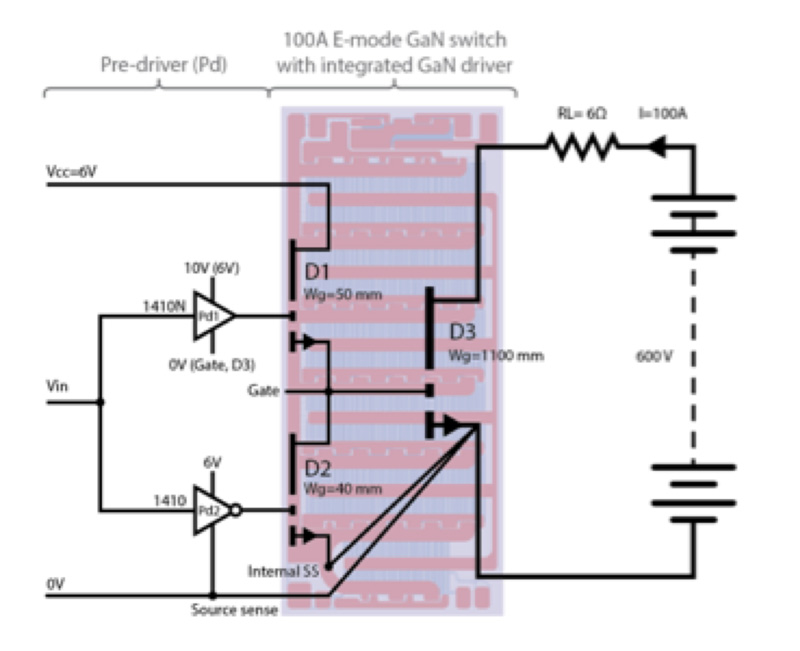
A better result can be achieved if an on-chip driver is provided. The circuit shown in Figure 1 uses two on-chip, normally-off GaN transistors D1 and D2 to drive the large transistor D3 (Gate width, Wg , of 1100 mm) on and off. In this circuit, the source sense loop is internal and very effective because of the very low loop inductance that is achieved.
Click image to enlarge
Figure 1: The source sense loop is internal and very effective because of the very low loop inductance that is achieved.
As a result of providing D1 and D2 on-chip, the external pre-driver devices can be far smaller than the drivers typically used for very high current power switches. The pre-drivers shown are the Microchip TC 1410 and TC 1410N devices. These are small devices rated to provide only 0.5A of output current, but they are however, ideal for use in this circuit because the required peak current is well within their 0.5A capability. If the D3 device was driven directly, a 10A peak current drive capability would be required and these large driver devices, with corresponding high current capability, also suffer from higher internal delays. Additionally, as noted previously, it is difficult to mount the large driver close enough to the large GaN transistor to eliminate loop inductance.
Any weakness in the drive circuitry can lead to excessive power dissipation during the on-off transitions as shown in the temperature-time chart of Figure 2. This chart shows that stable, thermal operation – or catastrophic thermal runaway, depends on the drive circuit design. Unsafe drive conditions occur when the internal D1 and D2 driver devices are not cleanly driven to clamp the gate of D3 rapidly, to either the 6V supply or the source sense connection.

Click image to enlarge
Figure 2: Safe drive condition provides stable operation
Drive issues therefore can limit GaN transistor performance. It is also vitally important to use sophisticated, thermally augmented SPICE models. However, these models cannot cope with the localized heating effects common in simple, conventional ladder layouts that produce hot spots in the center of large die. Standard, hot chuck testing will not reveal these characteristic limitations of the traditional ladder layout and they are definitely not revealed when using conventional SPICE models [1].
Island Technology
The Island Technology designs with numerous, totally independent cells shown in Figure 3, are compact, scalable and they more evenly spread heat over the whole die. The large area, GaN power switch with the on-chip drivers, can then be accurately simulated in conjunction with the models for the 1400 series pre-drivers provided by Microchip. This is an important practical requirement because GaN-on-Si devices are very challenging to thin below 250 µm. The Island Technology devices are far more easily modelled.
Click image to enlarge
Figure 3: Island Technology designs with numerous, totally independent cells
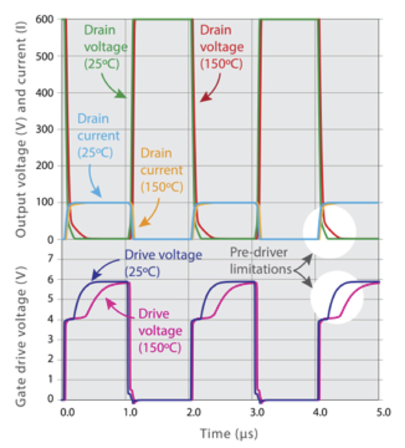
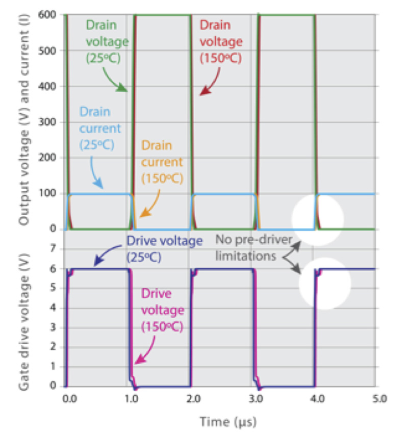
When the thermal models are correctly applied and the highly non-linear device capacitances are correctly represented, very complete and accurate simulations of the circuit shown in Figure 1 can be produced. The effect of providing a poor drive signal at the gate of D3 is shown in Figure 4a. The slow fall time of the 600V transistor is caused by the poor pre-driver transition also shown. However, when the drive signal is optimized, as shown in Figure 4b, the safe drive condition can be achieved, rather than the thermal runaway condition as shown in Figure 2. Clean drive signals to the on-chip drive transistors result in the smallest overlap of the output voltage and output current as shown in the highlighted sections of Figure 4 (a) and (b). Minimum losses occur when the smallest overlap is achieved.
Figure 4: Poor drive conditions result in excessive power loss (a). Good drive circuitry removes the major power loss (b). The highlighted sections display the difference.
Click image to enlarge
Click image to enlarge
Conclusion
The value of having on-chip drivers for very large, high power 650V GaN transistors with Wg of 1100mm, 1500mm and 3000mm has been described. These devices are suitable for drive train use in all classes of electric automobile types. For vehicles that require 1200V operation, three level inverter circuitry will be used because the 650V GaN devices will be the most prolific, low cost, high voltage devices available, replacing IGBTs and SJ MOSFETs. However, they initially need to be proven in the less demanding and disposable IT applications.
Manufacturing very large, high reliability, 650V devices with high yield is a challenge. However, the Island Technology allows for the required redundancy because the devices are made from numerous totally independent cells. For example, the 3000mm 400A device has 136 cells. The yield and reliability issues have been addressed by using this island layout technique. The drive problem has been solved by using the on-chip GaN driver.
References
1. J. Roberts, T. MacElwee, and L. Yushyna, "The Thermal Integrity of Integrated GaN Power Modules", IMAPS Conference & Exhibition on High Temperature Electronics Network (HiTEN 2013), July 8-10, 2013, Oxford, UK, pp.61-68.