Achieving high-power, low-loss switching
The quest for energy efficiency has focused attention on those components of the power electronics that can connect hundreds of volts and amps in inverters with exceptional efficiency. We are talking about modern power switches – IGBTs and SIC-FETs – and how the voltage supplied to the respective gate drivers is optimized.
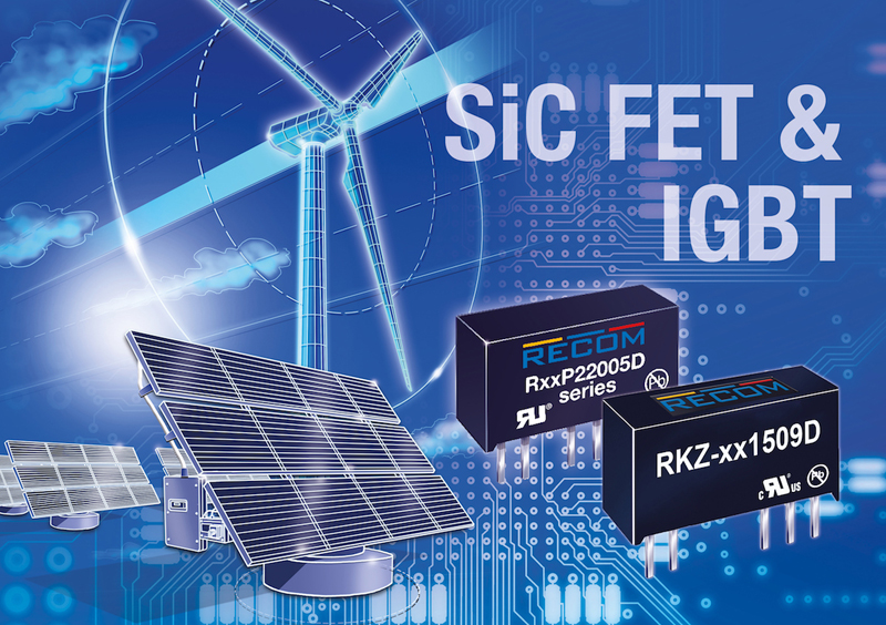
These semiconductor technologies are used across the entire spectrum of power electronics – from engine controllers through to welding systems, induction furnaces and vacuum generators all the way to electromobility, inverters for wind and solar energy generators and numerous other applications. As a result, they represent a core area of Rutronik’s power business (see Figure 1).
Click image to enlarge
Fig.1: Highly insulated DC/DC converters ensure optimum supply of power to IGBT and SiC-FET drivers used in power electronics. (source: Recom)
In the early phase of power electronics, developers only had access to bipolar power transistors. They were suitable for blocking voltages of up to 500 V and could switch currents of 100 amps and more. However, this impressive performance came at the expense of very high control currents to containing switching losses by using relatively steep edges. For this purpose, 10 to 20% of the collector current was required at the base.
This problem was overcome by the development of the first power MOSFETs (Metal-Oxide Silicon Field-Effect Transistors). The gate of MOSFETs is insulated, which means that only negligibly low currents are required to charge and discharge the gate capacitance. The energy loss during actuation was reduced significantly.
Naturally, two familiar sources of losses associated with bipolar semiconductors remained:
1. The "switching losses" caused by the limited edge steepness during the switchover cycles
2. The "conductive" losses in the conductive state of the semiconductor – also referred to as "ON losses"
Whereas the latter are defined by the technical specification of the MOSFET and are therefore largely fixed, the quality of actuation is primarily responsible for switching losses. The developer can use suitable switching concepts to influence this.
IGBTs combine the advantages of MOSFETs and bipolar transistors
With the development of IGBTs, it was possible to eliminate the disadvantage of higher "ON losses" via the drain-source connection. As the name "Insulated Gate Bipolar Transistor" implies, this involves a mixture of MOSFET at the input and a bipolar transistor at the output. In this case, the genes of both parent parts complement each other perfectly. As with MOSFETs, IGBTs can be activated with virtually no current. In their conductive state, they also exhibit the low voltage drop on the collector/emitter connection typical of bipolar transistors. Therefore, they are capable of switching high voltages and currents with very low losses.
SiC-FETs are ideal for higher outputs and frequencies
Whereas IGBTs are made of mono-crystalline silicon, SiC-FETs use silicon carbide. This material has a higher melting point and permits the use of significantly thinner insulation coatings at the gate. This not only improves thermal conductivity but also enables higher power density.
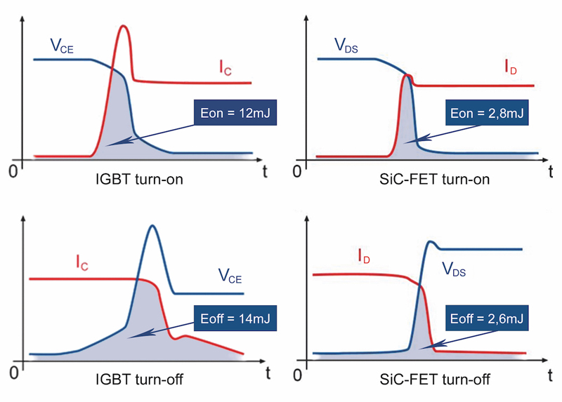
The switching losses of SiC-FETs are at least 4 times lower than IGBTs (see Figure 2) – an advantage that pays dividends particularly in the upper power range and at higher switching frequencies. However, the higher cost of SiC-FETs means that they will be concentrated primarily in the high-performance area for the near future and will not take the place of IGBTs in the mass market.
Click image to enlarge
Fig.2 : The area below the current/voltage curves during closing (upper diagrams) and opening (below) is an indication of the switching losses. Due to steeper switching edges, SiC-FETs (top right and below) are around 4 times more efficient than IGBTs – at a 25°C ambient temperature and taking body diode losses into account. (source: Recom)
Insulated DC/DC converters provide optimum power delivery
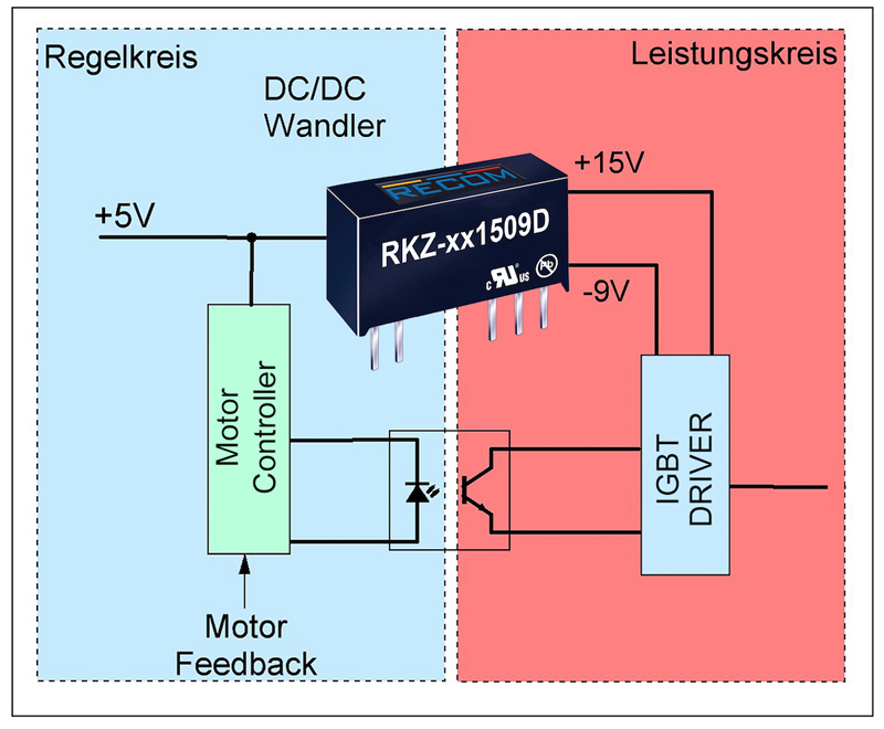
As mentioned above, switching losses are largely determined by the quality of actuation. For this reason, particular attention must be devoted to the gate drivers and their power supply. Since the drivers are directly coupled to the high potentials of the IGBTs or SiC-FETs, both the signal input and the voltage supply to the driver ICs must be very well insulated. The latter can be realized particularly conveniently with insulated DC/DC converters.
Standard commercial driver modules are asymmetrically actuated with positive and negative voltages. However, IGBT and SiC-FET drivers differ with regard to the voltage levels required. The data sheets for IGBTs specify a threshold voltage of +3 V. In practice, however, +15 V is generally required to ensure fast, clean conduction. To ensure reliable opening, it may even be necessary to set a negative bias at the gate in view of the high dV/dt load. This will prevent unintentional re-closing. In practice, a value of -9 volts has shown to be safe. In other words, converters with voltages of +15 volts and -9 volts are needed to supply IGBT drivers (see Figure 3 a).
Click image to enlarge
Fig.3 a & 3b: IGBT and SiC-FET drivers can be supplied with exceptional convenience by highly insulated DC/DC converters, provided that they are equipped with asymmetric outputs of +15 V/-9 V, or +20 V/-5 V. (source: Recom)
A slightly different situation arises in the case of the SiC-FET, whose switching threshold is around +1 to +2 V. To keep the conductive losses (RDSON) low, a gate-source voltage of +20 V is recommended. If one were to make do with the level of +15 V normally used for the IGBTs, the RDSON losses would be up to 30% higher! A value of -5 V has proven to be effective for reliable opening (see Figure 3 b). A higher negative voltage would lead to a change in the gate-source parameters and therefore to impaired stability.
High dv/dt puts pressure on insulation barriers
In the figurative sense, the insulation of a DC/DC converter can be compared to a dike that is designed to withstand a specific maximum level. If it is higher than the level of a storm tide, it will defy the waves. However, if the waves wash over at certain points, it is in danger of being breached at some stage.
The situation with the insulation of a DC/DC converter is very similar. High switching frequencies – for IGBTs, mostly 10 kHz to 50 kHz, for SiC-FETs, usually > 50 kHz – and steep edges place the insulating components in the system under permanent stress. Particularly in conjunction with "hidden", parasitic capacities and inductances in the circuit, voltage peaks can occur that the push the insulation of a converter to the limit. There are no "magic formulas" that can be used to precisely determine the level of the voltage peaks and therefore the life expectancy of the system.
Even measurement technology can only offer very limited assistance. That is because even the relatively low capacitance of the high-voltage scanning head of an oscilloscope will distort the measurement. For example, a voltage peak measured at 2 kV could in reality – without the load applied by the scanning head – be twice as high. There is no absolute certainty. Those who rely on measurement and use a converter with inadequate insulation are putting the long-term reliability of their products at risk. For this reason, developers tend to allow for sufficient safety reserves and use converters with the best possible insulation when designing rapid power switches.
For example, the Rutronik power portfolio includes DC/DC converters by RECOM specifically designed to supply IGBT and SiC-FET drivers. They have asymmetric outputs with a choice of either +15 V/-9 V (IGBT) or +20 V/-5 V (SiC-FET) at input voltages of 5 V, 12 V, 15 V and 24 V. The required power depends on the switching frequency, among other things. At around 10 kHz, power levels of up to 1 W are sufficient in most cases. At 50 kHz and higher, up to 2 W are required. The products operate in power-sharing mode, i.e., the nominal power can be distributed as required to the two outputs. Additional differences apply to the insulation. The RKZ family can be supplied with insulation voltages of 3 kV DC and 4 kV DC, the RxxP2xx versions even with high 5.2 kV DC voltages.