Author:
By: Eleazar Falco, FAE, Emil Nierges, Product Manager, Würth Elektronik eiSos
Date
10/01/2022
 PDF
PDF
Click image to enlarge
ÂIn power electronics, semiconductor transistors with a wide bandgap, such as silicon carbide or gallium nitride, are becoming increasingly popular. Higher switching speeds promise higher efficiency and higher power densities. Two reference designs from Würth Elektronik show how an isolated 6 W auxiliary power supply can be realized for SiC MOSFET & IGBT gate drivers.
Silicon Carbide (SiC) technology is enjoying growing popularity in medium and high voltage power switching applications (typically above 300 V). The extremely fast switching speed of SiC-MOSFETs, their low on-resistance and excellent thermal performance (conductivity and stability) are some of the key advantages against their Silicon-based counterparts. SiC devices are thus starting to replace silicon-based devices like IGBT (Insulated Gate Bipolar Transistor) and Power-MOSFETs in industries like E-mobility, industrial drives and renewable energy.
The voltage required across the gate-source terminals of a SiC-MOSFET are typically found in the range of 15 to 20 V for full turn-on and 0 to -5 V for robust turn-off. Note that a negative voltage is typically used for a faster turn-off transition as well as to keep the device off reliably, preventing spurious turn-on caused by parasitic resonant ringing or Miller-effect in hard-switched, half-bridge applications. This is caused by the very high dv/dt generated across the device terminals during fast switching transitions. A bipolar isolated auxiliary supply therefore provides a positive and a negative voltage. Some devices require a unipolar voltage instead, and reliable turn-off at fast switching speeds can be guaranteed by other means, for example, an active Miller Clamp. For both versions, bipolar [1] and unipolar [2], Würth Elektronik developed dedicated reference designs.
Gate Driver, SiC-MOSFET and Auxiliary Power Supply
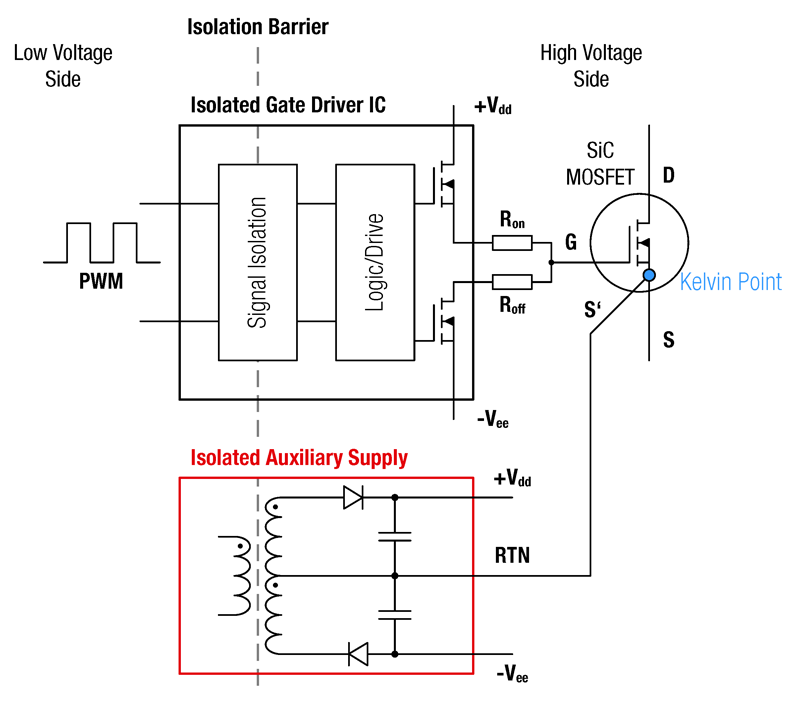
A low-power isolated auxiliary supply, typically a flyback, push-pull or half-bridge topology, provides the gate drive voltage level and power required to switch on and off the SiC device, in addition to the galvanic isolation between the high-voltage and low-voltage sides. Isolation is a requirement not only to meet relevant safety standards, but also to reduce electrical noise improving EMI and gate driver control robustness. The transformer in the auxiliary supply fulfils this primary task. Regarding the gate driver stage, an isolated gate driver IC with an output transistor stage in push-pull/totem-pole configuration is typically used to drive the gate-source of the SiC device based on a control signal from the controller system. The system connection is shown in figure 1.
Click image to enlarge
Figure 1: Connection of bipolar auxiliary supply with gate driver IC and SiC-MOSFET. In the unipolar case the lower loop with –Vee is dropped
It is important to note that some SiC devices feature an additional Kelvin pin S’ for the source terminal, as shown in the circuit diagram. This connection provides a dedicated Gate-Source path for the gate drive current, which is not ‘shared’ with the current of the power loop (Drain-Source) at the source terminal. This prevents common-source inductance issues during fast switching transitions, caused by the high dI/dt of the power loop current causing a voltage drop across the source parasitic inductance, which opposes the applied gate drive voltage, slowing down the switching speed. The isolated ground of the auxiliary supply (RTN) must be connected to this terminal if available, as shown.
Bipolar versus Unipolar
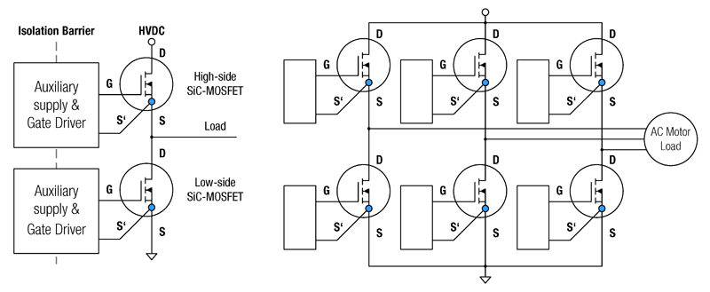
A half-bridge configuration is the building block of many switching power converters (figure 2 left), with a high-side and a low-side SiC-MOSFET device switching alternately. Each transistor typically has its own auxiliary power supply and gate driver circuit.
Click image to enlarge
Figure 2: SiC-MOSFET half-bridge configuration (left) and 3-phase inverter application example (right)
When the high-side SiC device is turning on, the complementary low-side SiC device is already turned off as ‘dead time’ is used. Dead time is a short time window during switching transitions where both devices are kept off in order to prevent shoot-through or cross-conduction. This is caused by both devices being turned on at the same time due to control signal propagation delay mismatch in the gate driver, parasitic ringing, etc.
By holding the gate-source connection to a negative voltage, extended margin to the SiC-MOSFET turn-on threshold voltage (Vth) is provided. This additional headroom can help to prevent spurious turn-on due to Miller-effect and/or parasitic ringing during the very fast switching transitions, and in addition to increase the switching speed. If only a unipolar gate drive voltage can be used due to particular system requirements, an active Miller clamp could solve the issue.
The active Miller clamp, in its simplest form, consists of a transistor connected right across the gate and source terminals of the SiC device and a simple control circuit. The Miller clamp can be implemented either externally with discrete components or by using a gate driver IC with embedded active clamp circuitry. The principle of operation is simple: the control circuit ‘monitors’ the gate-source voltage and turns on the clamp transistor when it drops below a threshold level during the turn-off transition. In this way, a very low impedance path for the Miller current is provided, since the transistor is in parallel with Zgs, and it would ‘ideally’ bypass the parasitic elements across the gate-source terminals and thus shunt most of the Miller current caused by the high dv/dt.
Auxiliary Supply - Output Power
During the switching transitions of the SiC-MOSFET device, power is dissipated in the gate current loop resistance as current flows to charge and discharge the gate capacitance of the device to the positive and negative auxiliary supply voltage levels, in order to turn it on and off respectively. The auxiliary supply of the gate driver system needs to source this power, which depends on the gate voltage, switching frequency and total gate charge of the SiC-MOSFET.
Isolation Barrier Parasitic Capacitance and CMTI
CMTI is the acronym for ‘Common-mode Transient Immunity’, and it is measured in kV/µs or V/ns. It is an indication of the maximum rate of change of voltage (dv/dt) which can be tolerated across the isolation barrier of the gate driver system before malfunction occurs, causing loss of control of the SiC device and erratic behavior of the system. The CMTI rating directly depends on the parasitic capacitance value across the isolation barrier.
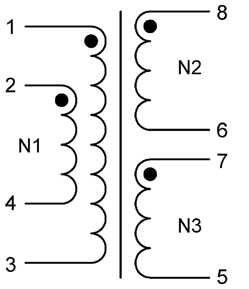
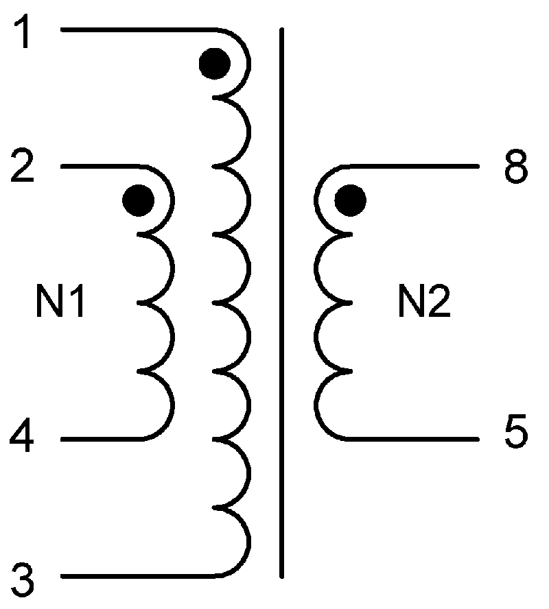
The transformer series WE-AGDT from Würth Elektronik feature a very low interwinding capacitance down to 6.8 pF, helping the gate driver system to achieve CMTI ratings above 100 kV/µs. These are designed for optimal characteristics to be used in PSR Flyback converter reference designs to drive high-performance SiC-MOSFET devices, providing the most commonly required gate drive voltages (figure 3).
Click image to enlarge
Figure 3a: Dual-Output Transformer of the WE-AGDT series for bipolar topologies
Click image to enlarge
Figure 3b: Single-Output Transformer of the WE-AGDT series for unipolar topologies

Click image to enlarge
Figure 3c: WE-AGDT Transformer series
Finding an optimal converter operating condition to achieve the smallest transformer size and at the same time high efficiency, good thermal performance and compliance with relevant safety standards were the key design objectives. The WE-AGDT 750318131, 750319496 and 750319497 transformers use a very compact EP7 assembly, 4 kV isolation voltage, overvoltage category II, pollution degree 2, fully insulated wire (FIW) and creepage/clearance distances according to standards IEC62368-1 and IEC61558-2-16. Additionally, it complies with AEC-Q200.
Reference Design
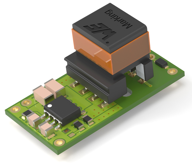
The two reference designs (figure 4) present extremely compact auxiliary power supplies with a combined output power of up to 6 W. RD001 [1] provides three different isolated bipolar output voltages: +15 V / -4 V, +19 V / -4 V and +20 V / -5 V, whereas the unipolar version RD002 [2] offers output voltages adjustable between +15 V and +20 V, while covering an input voltage range from 9 to 18 V.
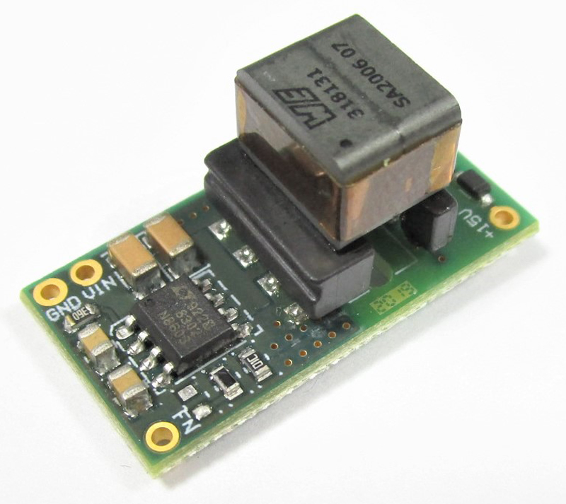
Click image to enlarge
Figure 4: Reference Design for an isolated auxiliary power supply with Gate-Driver-IC LT8302 from ADI and transformer WE-AGDT from Würth Elektronik
Key Features of the reference designs RD001 and RD002 with WE-AGDT transformer:
References
[1] Reference Design RD001 – 6W bipolar isolated auxiliary supply for SiC-MOSFET & IGBT gate driver: https://www.we-online.com/RD001
[2] Reference Design RD002 – 6W unipolar isolated auxiliary supply for SiC-MOSFET & IGBT gate driver: https://www.we-online.com/RD002
[3] Data Sheet of the transformer series WE-AGDT from Würth Elektronik: https://www.we-online.com/AGDT