In today’s data acquisition systems (DAQs), performance boundaries are continually being pushed. System designers require higher speed, lower noise, and better total harmonic distortion (THD) performance; all of which are possible but none of which are free. These performance improvements typically come at the cost of higher operating currents, which in turn result in greater power dissipation. However, in many applications sensitivity to power consumption is also an ever-increasing concern.
The reasons are varied. It may be a remote system operating from a coin cell battery where the primary concern is battery life, or perhaps a multi-channel system where the concentration of heat from high channel count and high circuit density can add up to temperature induced drift problems. In either case, minimizing current draw and power dissipation is of paramount importance. The system designer must strike a balance between the competing priorities of higher performance and lower power consumption. One path toward a solution is through a process called dynamic power scaling (DPS).
What is it?
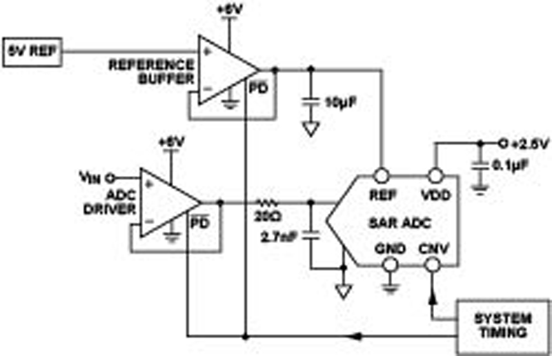
Simply stated, DPS is the process of dynamically enabling an electronic component when it is needed and disabling it when it is not. Figure 1 shows a typical SAR ADC based data acquisition sub-system. One of the key attributes of the SAR ADC is that its power scales with the throughput rate, making it a very attractive option for power sensitive applications.
Click image to enlarge
Figure 1. Block Diagram of SAR ADC Based Data Acquisition Sub-system
Historically, the ADC driver and reference buffer have not shared the automatic power scaling enjoyed by the SAR. They are typically powered up and enabled any time the system is running, thus consuming excess power. Assuming a sufficiently fast enable time, the amplifier power down pin can be dynamically driven to disable the amplifier between ADC conversions. This is dynamic power scaling (DPS).
By applying DPS to the amplifier its average current draw can be greatly reduced. With DPS the amplifier quiescent current is a function of the duty cycle with which the power down pin is being driven.
The theoretical average quiescent current is given by
Where:
IAVG is the average DPS quiescent current
IQ_ON is the quiescent current of the amplifier enabled
IQ_OFF is the quiescent current of the amplifier disabled
tON is the time the amplifier is enabled
tS is the sampling frequency period
We are using the ADC driver amplifier as our example, but these DPS concepts can be applied to the reference buffer with similar results.
Efficiency
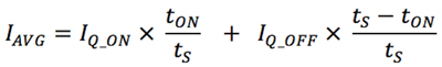
Figure 2 shows the theoretical efficiency improvements in amplifier quiescent power possible through DPS for a typical 16-18-bit amplifier/SAR ADC combination. In this generic example the horizontal reference line at 100% represents the power consumption of the ADC driver amplifier when it is constantly enabled. The vertical reference line at fR represents the sampling frequency at which the power consumption of the ADC equals that of the constantly enabled driver amplifier.
Clcik image to enlarge
Figure 2. Theoretical amplifier power consumption for DPS at selected tON (relative to amplifier constantly enabled)
At lower sample rates the amplifier dominates the power consumption and at higher sample rates the ADC dominates. The reference frequency (fR) will vary depending on the power consumption of the amplifier and ADC chosen but the basic concepts remain the same. The relative efficiency improvements for the same amplifier being power scaled are shown for three different values of tON. As expected a shorter tON results in greater efficiency at a given sample rate and enables the use of DPS at higher sample rates.
The shaded region shows that the area of greatest improvement for incremental shortening of tON generally extends down to about one decade below fR. As the sample rate continues to decrease below that point, the greatest overall power savings is realized, but the added benefit of further shortening tON is negligible as the power consumption asymptotically approaches that of the power down or disabled state. To achieve optimum performance with DPS, system timing and determination of minimum tON are critical.
Figure 3 shows a simplified timing diagram for the ADC and driver amplifier. The system timing block (FPGA, DSP, µcontroller, etc.) from Figure 1 provides the properly timed ADC conversion start (CNV) and amplifier power down (PD) signals. The SAR ADC initiates a conversion on the rising edge of CNV. The amplifier is powered on during the ADC acquisition phase for some period of time (tON) prior to the rising edge of CNV, and is then powered down synchronous with the rising edge of CNV. But what is the correct period of time for tON?

Click mage to enlarge
Figure 3. Simplified Timing Diagram for Amplifier and ADC Control Signals
While Figure 2 illustrates the concept using somewhat arbitrary times for tON it clearly shows that the full value in DPS will be realized only when the minimum tON is used. This is the minimum time for which the amplifier must be enabled prior to the ADC conversion to ensure an accurate result. Any time shorter than this will result in erosion of SNR or THD while any time longer will not result in any performance improvements. In practice the minimum tON is not constant across sample rates and must be empirically determined for the unique application. The minimum tON will vary from amplifier to amplifier and system to system.
For example, using an amplifier/ADC combination of the ADA4805-1 and AD7980 in the circuit of Figure 1, the minimum tON decreases with increasing sample rate, typically requiring ~4 us at 1 ksps and only ~600 ns at 1 Msps. At low sample rates the long period provides more time for internal amplifier nodes to discharge due to an extended time in the power down state, resulting in longer turn-on time.
Conversely, the shorter period of higher sample rates doesn’t allow for as much internal discharging. In fact, as sample rate increases the finite turn-off time of the amplifier will become longer than the time spent in the power down state. In effect, the amplifier is turning back on before it has finished turning off. This gives the appearance of an artificially fast turn-on time but is validated when performance data shows no degradation.
Input signal frequency
One final point to consider when predicting potential power savings is the effect of the input signal frequency. Thus far the concept of DPS has been illustrated using the calculated quiescent current of a given amplifier. With a signal applied to the amplifier input, there will also be dynamic current that increases with the input signal frequency. If the input frequency is low enough the effect is inconsequential. As the frequency increases the RC network at the amplifier output presents a heavier load, requiring more current from the amplifier to process the signal.
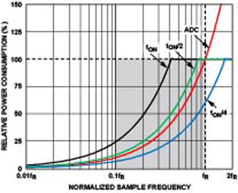
Using the ADA4805-1 and AD7980 mentioned above and putting this all together yields the curves in Figure 4. This figure shows the power consumption, in percent, of the dynamically power scaled ADC driver amplifier relative to the same amplifier when constantly enabled. The DPS efficiency is plotted for selected input frequencies to illustrate the effect of higher input frequencies on power consumption. The minimum tON was determined for multiple sample rates from 1 ksps to 1 Msps and is defined as the shortest tON that results in <0.5dB erosion in SINAD (signal to noise and distortion) from the case with the amplifier constantly enabled.
Click image to enlarge
Figure 4. Relative Amplifier Power with Dynamic Power Scaling, Experimental Results
The figure shows that power savings up to 95% can be realized when processing slow input signals at low sample rates. But perhaps more importantly, for higher throughput systems the potential savings is still significant, up to 65% at 100 ksps and up to 35% at 1 Msps. It is important to note that Figure 4 reflects the performance of a single unity gain buffer in a continuously sampled system. However, as previously stated, these DPS concepts can be readily applied to the reference buffer with the expectation of similar results.
While DPS is a relatively new concept, and there are design and timing considerations to take into account, the initial results are promising. One thing is very clear, the desire for higher performance and lower power consumption will continue into the future, which will further increase the need for creative low power solutions.