Eco-Sustainability Using Pressure-less Silver Sintering
Efficient performance and superior bonding technology that meets growing and diverging packaging needs
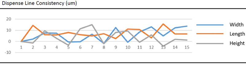
Figure 1. Dispense Line Consistency (um)
Silver sintering provides a void-free strong bond with superior thermal and electrical conductivity. It can decrease the junction temperature (Tj) of a device up to 100°C. In the process, when the material is heated under optimal pressure, temperature and time, its form will change from powder to a solid structure. The result is greater reliability, significantly increased performance and longevity, simultaneously being more energy efficient and placing less stress on the package. In summary, the process offers a performance that surpasses traditional sintering, while meeting the needs of rapidly growing market demand, 5G, evolving technologies, issues of energy conservation, eco-sustainability and lead-free requirements.
Ag sintering
Ag sintering works well with wide-band gap materials such as GaN and SiC due to its temperature capability (c. 500ºC). When combining GaN die on SiC substrates and using Ag sintering to make the bond, the lower temperatures will result in less residual stress while retaining high operating temperatures. In addition, silver offers excellent thermal and electrical performance and represents marginal material cost while offering lower, energy saving temperature sintering. As to the bonding process itself, inherent physical and commercial advantages include the fact that it can be sintered in the presence of air and can be dispensed using the same set of tools and with a similar procedure as solder paste; cost-wise a straight-forward “drop-in” solution.
Case Study
The work was undertaken at Palomar’s Innovation Center in Singapore using a Palomar 3880 Die Bonder and a “drop-in” Musashi jet dispenser in the Class 100k clean room with locally sourced materials.
To ensure the material volume was consistent and the process was repeatable and void free, it was critical to ensure the development of a controlled, highly accurate, consistent bond line thickness (BLT) that delivered a uniform adhesive layer delivered across the bonded area. “Critical” because even small inconsistencies produced peel stresses resulting in reduced adhesion strengths. A line that is too thick ( >50 μm) results in increased resistance negatively affecting electrical performance. Overly thin bond lines (<30 μm), on the other hand, results in voids, adhesive starvation and de-bonding—all undermining long-term device performance.
Other requirements included compensation and control which in turn demanded an effective metrology. Gauging bond line thickness can be variously achieved. Regardless of the method, bond line thickness should be measured—as it was here—at different positions to evaluate uniformity. Equally important is a consistently flat surface that includes sufficient roughness for an accurate, correct and repeatable BLT. Our method for verification was to use confocal microscopy to provide a visual and qualitative measurement of the surface.
Jet Dispensing
A non-contact jet hovered over the location dispensing adhesive dots at high speeds from a height between 1mm and 3mm above the surface. This inherently minimized adhesive tailing allowed for tighter pitch, deeper access and reduced chances of damaging the die. No alternative pump method could deliver this level of performance. Moreover, the Z-axis motion was eliminated during dispensing, yielding a factor 10 increase in process speed (1000 dots/min). The mechanics of the jet dispenser made it possible to program different sized dots and to jet multiple shots in the same location. With a temperature controlling system integrated into the jet pump assembly, optimal viscosity was successfully maintained.
OUR Sintering Process
In terms of the exact sequence:
• Coupon loaded onto the presentation stage and vacuum clamped.
• Touch-tool height measured.
• Ag sinter dispensed on bonding from a height of 127 μm.
• Customized pickup tool moves GaN die to sintered location/substrate.
• GaN die placed using Fixed Height BLT technology.
• Coupon removed and wet (before sinter) BLT measurement secured.
• Curing ramped from 25°C to 210°C and soaked for 60 minutes.
• Measured for dry (after sinter) BLT.
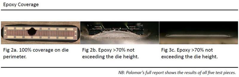
Five GaN dies were processed at 90-minute intervals. Standard applications of bond force, axis speed, etc., were applied to pick and place the GaN die while adhering to height parameters in the 35-50 μm range. A total of 15 lines were dispensed on the coupon/substrate. Measurement followed immediately upon completion. The results demonstrated a width, length and height consistency within the 15 μm tolerance range and well within our specification of 25.4 μm. Figure 1 shows the results of the Ag sintering lines jet dispense using a Musashi AeroJET. Figure 2 illustrates how we successfully achieved 100% epoxy coverage to 70% of the die height.
Central to this process was Palomar’s bespoke software program which precisely controlled the dispense of the Ag Sintering material and subsequent bond/process activities.
Click image to enlarge
Figure 2. Epoxy Coverage
Click image to enlarge
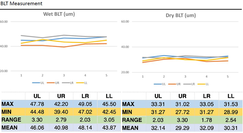
Figure 3. BLT Measurement
3D confocal microscopy allowed measurement of the corner top surface of the die to establish bonding height after cure; beginning with the surface height from the center where the die placement would follow. There were no further touches to the substrate surface—and thus no potential threats of physical damage. The die thickness (108.4263 μm) was subtracted from the die height to get the effective BLT. The results show (Figure 3) the specification of a wet BLT of 42.5 μm ±7.5 μm and a dry BLT of 27.5 μm ±7.5 μm was achieved. Measurements are shown for upper left, upper right, lower right and lower left of the bonded coupon. Void-free attainment was confirmed using a Sonix HS-1000 C-Mode Scanning Acoustic Microscopy (C-SAM) equipped with a 75 MHz transducer. The TAMI region was set from the surface of the coupon up to the GaN die with a 1.882 μm step resolution.
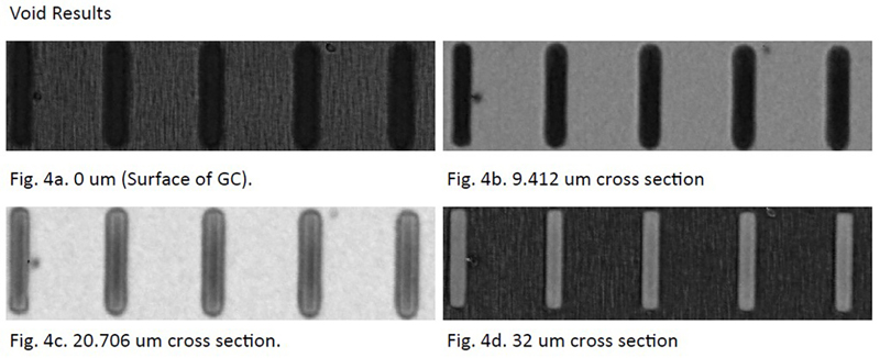
The images in Figure 4 present a typical sample of results at 18 different depths (0 μm to 32 μm) across the 5 units. No voids were present at any of these depths.
Click image to enlarge
Figure 4. Void Results
CONCLUSION
This case study—which we built on those undertaken previously— was prompted by several critical industry issues beginning with the imperatives of lead-free manufacturing and eco-energy consumption (efficiency and sustainability), then focusing on the engineering and process challenges required by successfully meeting cost and competitive pressures and exponentially evolving technologies. These studies allowed us to establish the following as critical factors as validating theprocess undertaken:
1. Highly critical invariability of the required bond height (+/-7.5 um).
2. Void free sinter bond line.
3. Accurate metrology.
4. Volume and repeatability.
5. Commercial sustainability.
As to the process itself all the key metrics including exceptional accuracy in maintaining the volume of the Ag Sintering material even after a few hours of the material being thawed. Moreover, the line consistency, epoxy coverage and delivery speed improvements over and against those attained by alternate methods (used but not cited in this article) were remarkable.
Other key successes included ease of use, effectiveness, accuracy and repeatability, volume potential, environmental constraints, energy consumption, and scalable dynamic engagement with new technology and packaging needs.


