USB standard has been updated to version 3.1
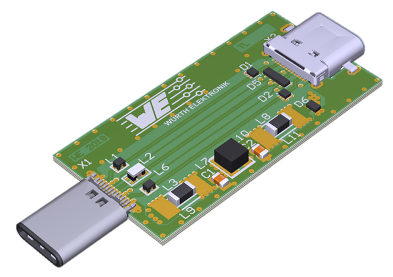
Figure 1: USB-C dongle used to demonstrate USB 3.1 filtering and protection
The USB connector and standard are one of the most widely implemented and successful interfaces ever used. The applications are commercial and industrial, and both have been pushing the standard to be faster. The USB standard has been updated to version 3.1. This standard increases data transfer speeds to 5 GBits/s (Gen 1) and 10 GBit/s (Gen 2). Higher data transfer speeds are required due to the ever-increasing resolution of media and network data rate requirements.
Increasing the data transfer speed means important parameters need to be considered, as this has implications in data transmission lines. Attenuating unwanted signals while maintaining the speed and integrity of data transfer is of paramount importance for EMI compatibility. For high-speed data lines, Würth Elektronik has common mode chokes for EMI suppression and TVS diodes for ESD protection. The WE-CNSW HF has been developed to attenuate common mode noise signals while maintaining signal integrity up to 10 GBit/s. For ESD protection, the WE-TVS is available with very low capacitances (< 0.6 pF) and is the ideal choice for higher frequencies. These components are also well suited for other high data transfer interfaces such as HDMI 4K, DisplayPort or GBit LAN. This component, among others, have been included in a filter designed to protect USB 3.1 devices and attenuate EMI that may cause the device to fail EMC testing (Figure 1)
EMI considerations of symmetrical data lines
The USB interface is a bidirectional, symmetric interface. VDM, interference voltage between the signal wires, and VCM,interference voltage between the voltage midpoint and the reference voltage (ground, cable shield), are both measurable. This means that both differential mode and common mode interference voltages can affect the USB transmission path. This can be interference from the interface itself or an electromagnetic effect from the environment in the form of inductive, capacitive or wave coupling.
In the case of USB transmission, differential mode interference is mainly generated by non-linear signal harmonics due to impedance mismatching and inadequate circuit design. Asymmetry of the transmission path (e.g. transmitter, circuit board traces, conductor tracks, filters or cables) can lead to interference radiation and impairment of signal quality.
Common mode interference arises from parasitic coupling in the circuit environment of the USB controller. This is usually due to capacitive coupling on the USB signal with rising interference frequency and increasing amplitude. However, these interference types are found on both USB wires in phase and at the same amplitude and therefore the effect on the intended signal is reduced. Asymmetries in the cable or at the receiver often convert the originally common mode into a differential mode interference signal, however, which can then contribute to signal impairment.
USB Type-C Dongle
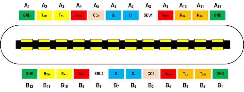
Modern demands have been pushing for a universal serial bus (USB) to be smaller, thinner and lighter. The USB Type-C connector was developed in parallel with the USB 3.1 standard (SuperSpeed+, USB 3.1 Gen 2), which is the updated standard of USB 3.0 (now USB 3.1 Gen 1). The connector now includes 24 pins (Figure 2) which include four power/ground pairs, two differential pairs (non-SuperSpeed+) and four SuperSpeed+ pairs (two used for USB 3.1). USB Type-C has data rates of up to 10 Gbit/s using one SuperSpeed+ and two SuperSpeed line pairs and can carry up to 5 A (100 W). To maintain signal integrity at these speeds, the capacitance of ESD devices must be even lower than that for USB 2.0 while CMCs need to present impedance to differential mode noise at higher frequencies.
Click image to enlarge
Figure 2: USB Type-C pin layout
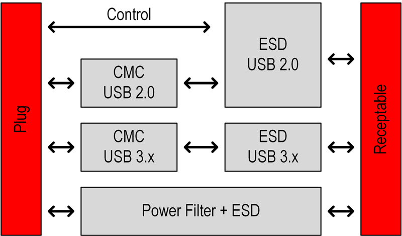
From the above pin layout, the power pairs are A1/A4, A9/A12, B1/B4 and B9/B12, the SuperSpeed+ pairs A2/A3/B10/B11 and A10/A11/B2/B3 and the non-SuperSpeed+ A6/A7 and B6/B7. These three functions can be treated separately and the necessary protection and filtering can be seen below (Figure 3).
Click image here to enlarge
Figure 3: Block diagram of the USB Type-C dongle
Additionally, A5/B5 are used to detect the connection and configure the interface. A8/B8 can be used for audio or additional features that have yet to be designated.
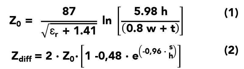
The nominal differential impedance of USB 3.1 data lines is 90 Ω, which must be maintained in the differential microstrip of the dongle. Z0 is calculated using the standard microstrip formula (1). To achieve impedance matching, the trace width w and height t, the trace separation distance s of the differential data traces in addition to the PCB permittivity and thickness h must be considered (Equation 2).
Click image to enlarge
USB 3.1 power channels
As previously stated, the power bus of the USB Type-C connector can handle up to 100 W (20 V / 5 A) when the cable is rated to such power. However, most applications will not use this high power capability. Therefore, the power bus filter must be designed to tolerate the power to be used by the application.
The USB 3.1 standard states a data rate of to 5 GBits/s (Gen 1) and 10 GBit/s (Gen 2). To attenuate any high frequency noise coupling to the power line, a low pass filter can be used with a cut-off frequency of approximately 1/10th of the data rate.
100 W (20 V / 5 A) applications
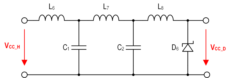
The WE-MSPB (742 792 261 01) ferrite has its maximum impedance in the range from approximately 100 MHz to 1000 MHz in which the highest level of interference is to be anticipated in USB data transmission. At 750 MHz the ferrite acts like an ohmic resistor with no reactive components. Above this resonance frequency, the capacitive behavior dominates the impedance. Additionally, a filter is required to bypass any additional high frequency noise. A π-filter was chosen as they have a high insertion loss because both the source and the sink in the power supply are of low impedance. This gives rise to an optimal mismatch and therefore maximum suppression. The following filter was implemented using well-known filter equations.
Click image to enlarge
Figure 4: Implemented SMD ferrites, π-filter and TVS diode topology for 100 W power capability
Click image to enlarge
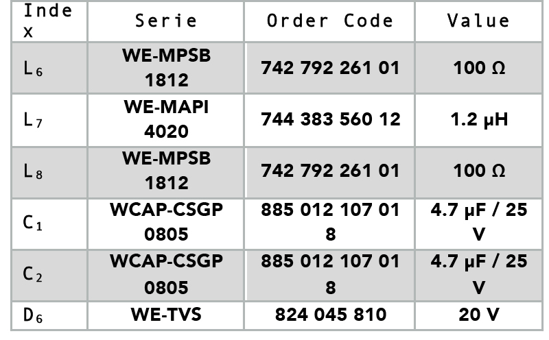
Table 1: Selected components for the 100 W design
60 W (20 V / 3 A) Applications
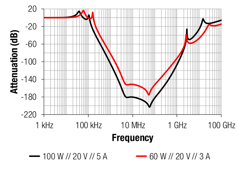
As a specialized cable is needed to handle 100 W of power, most applications will use 60 W or lower, which is the highest rated power of a ‘normal’ cable. Therefore, it may not be necessary to implement a filter that can handle 100 W. The following filter is implemented in a similar way to the 100 W filter but uses components with lower current handling capability and therefore, a more compact design.
Click image to enlarge
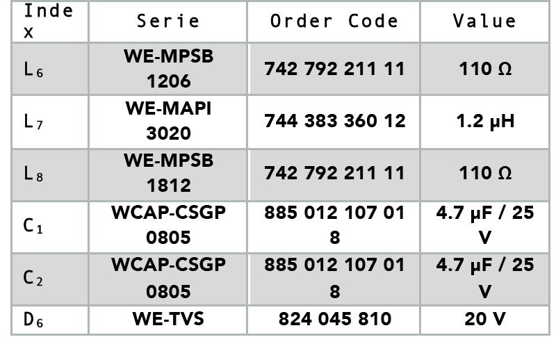
Table 2: Selected components for the 60 W design
Click image to enlarge
Figure 5: Simulated attenuation of the power line filter rated for 60 W and 100 W in comparison
USB 3.1 SuperSpeed+ channels
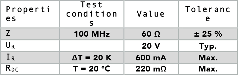
The WE-CNSW HF (744 233 56 00) is the heart of the data line filter. On account of its winding technology, the WE-CNSW HF has a high degree of symmetry and low parasitic capacitances. The most important parameters are given in Table 3.
Click image to enlarge
Table 3: Electrical characteristics of the current-compensated choke (744 233 56 00)
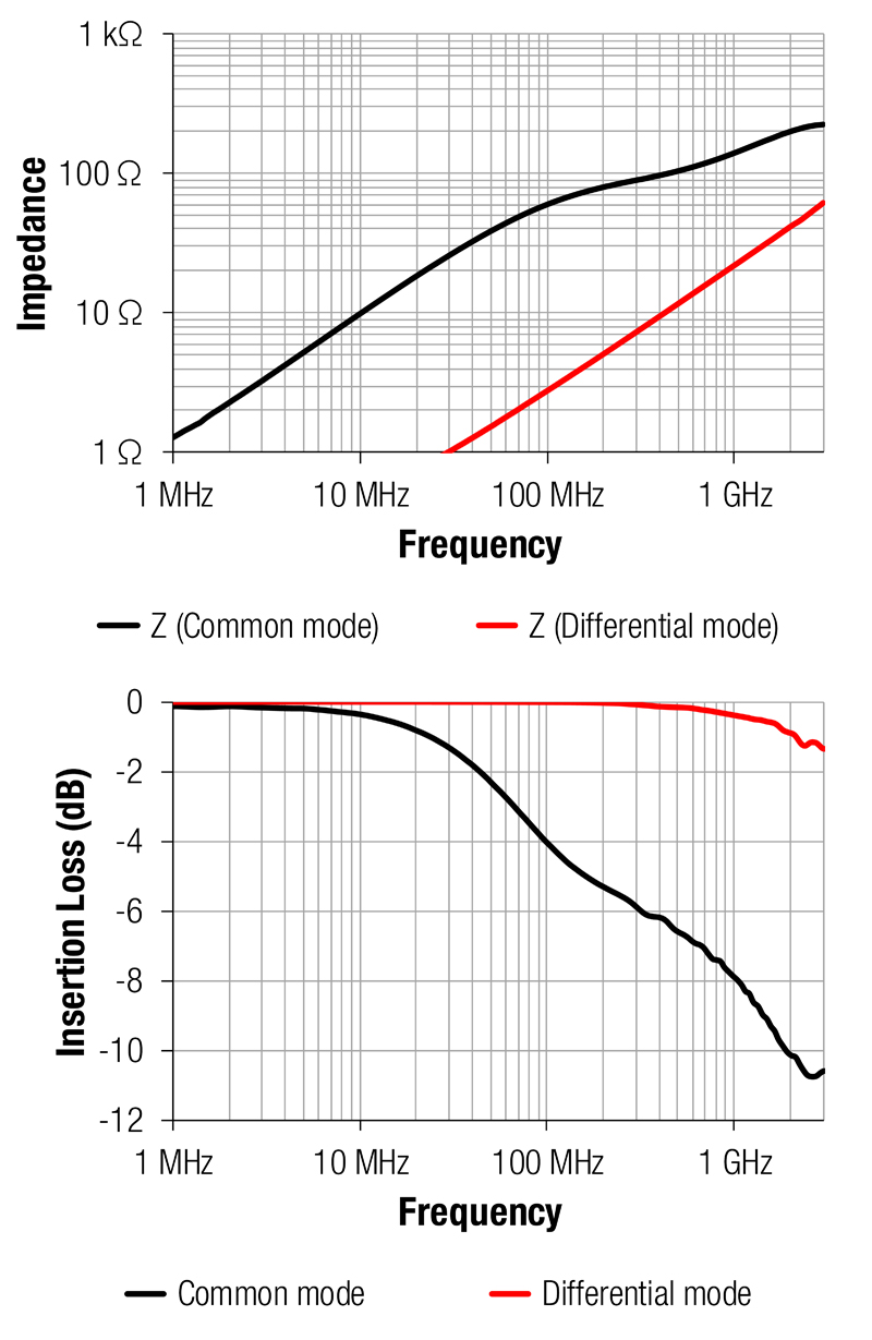
The impedance curve and insertion loss of the CMC in common and differential mode is presented in Figure 6. Common mode noise occurs when the same interference components propagate in the same direction on the positive and negative channels with respect to ground. This is always the case for capacitive or inductive coupling on the circuit or its conductor tracks. Therefore, this impedance component must be as high as possible. At 100 MHz the CMC has around 60 Ω. The differential mode impedance occurs due to the stray inductance of the winding structure. This impedance must be as small as possible at the data frequency.
Click image to enlarge
Figure 6: Impedance curve and insertion loss of WE-CNSW HF @ 50 Ω (744 233 56 00)
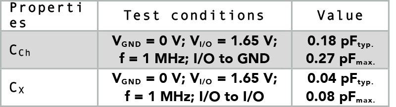
Including capacitance in the filter forms a low-pass second order filter. A diode array is used here instead of capacitors. The integrated diodes also have a parasitic capacitance, which can be effectively used. In addition, the parasitic inductance of the TVS diodes in the array is very low. This is necessary to attain a short response time to the overvoltage transients. Therefore, an almost ideal capacitor is combined with effective transient protection. The most important electrical characteristics of the array are presented in Table 4 .
Click imag to enlarge
Table 4: Electrical characteristics of the WE-TVS Super Speed Series (824 012 823)
Measurement
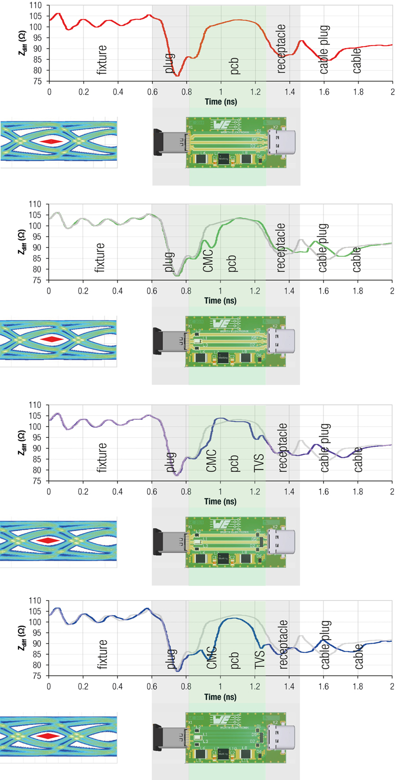
The test setup (1m cable and the type C dongle) was connected to the analyzer by a measuring fixture. The respective eye diagrams were taken at 5 GBit/s (USB 3.1 Gen 1). Figure 8a,b,c & d shows the variation of the differential impedance Zdiff in a time domain reflectometry (TDR). Here you can see well the slightly too high PCB impedance, which is caused by a pool board without impedance-controlled manufacturing.
When components are added to the PCB, the effect on the signal can be observed. The gray line corresponds to the measurement of an unpopulated PCB (see Figure 8). The first measurement includes the CMC, the second the TVS diodes and the third shows the effect when the solder mask is applied.
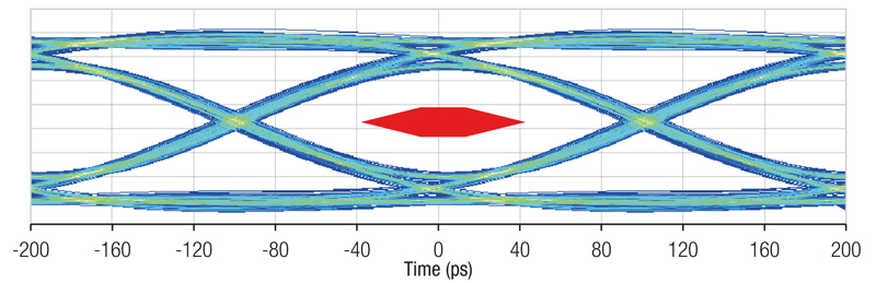
The basis for the measurement at 10 GBit/s is the adapter with all components and solder resist (Figure 7). The receiver can open the eye cleanly with the USB equalizer settings based upon the USB 3.1 r1.0 specification. Thus, a transmission with all protection components and connectors is well possible. With optimized components, you can achieve better results in advance and thus increase the range. The eye pattern test shows that the WE-TVSand WE-CNSW HF do not disturb the USB 3.1 signal.
Click image to enlarge
Figure 7: Eye diagram of the dongle with activated USB equalizer (@ 10 GBit/s)
Click image to enlarge
Figure 8a, b, c, & d: Time domain measurements and eye diagram of USB Type-C dongle without protection
Interface design kit
To facilitate the design of interfaces, Würth Elektronik has launched a dedicated Interface Design Kit (744 999). This design kit includes a design guide for USB 2.0 to USB 3.1, HDMI, CAN, Ethernet (100 and 1000 Base-T), VGA, DVI, RS232, RS485 interfaces and all the components used. These are ESD suppressors, SMD common mode chokes, chip bead ferrites, LAN transformers and the corresponding connectors. The color scheme makes it easy to locate the suitable parts for your application. Just follow the specific application color and select the suitable parts. For each application, there is a simple block schematic, which shows how to place the different components to get the best result.