Efficiency that Scores - USB-PD Solutions: Part 2 of 4
A digital forced quasi-resonant 65W high-density USB-PD design
Avoid complexity, incompatibility and shorten time-to-market! Infineon with its broad portfolio of high-performing and high-quality USB-PD solutions help engineers break through the barriers in fast charging designs at a competitive cost.
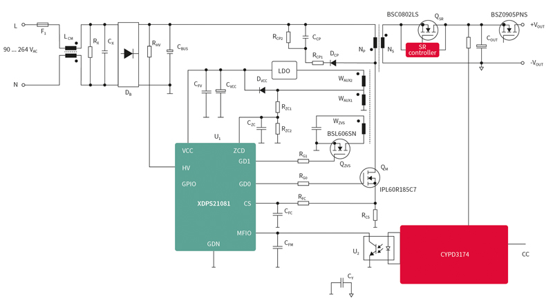
The solution introduced in this article is based on a digital zero-voltage-switching (ZVS) controller – the XDPS21081 platform, which achieves 21 W/in3 uncased power density. This 65 W reference design uses a universal AC input and converts it to the typical 5 to 20 V DC output supported by the USB-PD 3.0 protocol which is widely used in most modern laptops and smartphones. Using the resonant switching transitions virtually eliminates the main MOSFET switching losses in the desired frequency band. This approach can achieve the high switching frequency required to allow the use of smaller components (i.e., transformers), while still maintaining (or even improving) the efficiency required to manage heat dissipation in a very small form factor. In short, in all load and line ranges, the overall efficiency can be increased to more than 90 percent, and the peak efficiency can reach more than 93 percent.
It’s already here: a 65 W charger reference design for USB-PD application
The solution accepts a wide input range from 90 V AC to 265 V AC, and the output can vary from 5 V to 20 V, while the maximum output power is 65 W. A flyback topology and commodity components are selected to balance several factors such as cost, performance, or production. ZVS is enabled by an additional ZVS winding and ZVS circuit driven by the PWM controller XDPS21081 GD1 pin.
With the help of the ZVS function, the switching loss at high line is significantly reduced, so the switching frequency can be set at about 140 kHz. For low-voltage lines, the system operates in quasi-resonant (QR) mode under heavy load, thereby producing a natural ZVS effect to reduce power loss. Frequency-reduction mode (FRM) and active burst mode (ABM) are implemented to maintain high efficiency at medium- and light loads. Figure 2 shows the efficiency under different conditions.

Click image to enlarge
Figure 2: Four-point efficiency, surpass regulation requirements
One can activate brown-in and brown-out by connecting a resistor between the XDPS21081 HV pin and the bulk capacitor. In addition, the design has various protection features, such as, for example, OCP, Vout OVP, VCC OVP, OLP, OTP, latch enable, and CS-pin short protection before power-on.
The topology of choice for fast charger designs
Due to its cost-performance ratio, quasi-resonant flyback topology is widely used in the charger market. With this topology, valley switching can reduce switching losses and this single-magnetic-component topology can also bring cost advantages. Although the QR needs to be improved with the increase of power of the charger, the zero voltage turn-on in the full voltage input range cannot be guaranteed. Especially during the high voltage input period, the high VDS of the MOSFET results in significant switching power loss hence high-frequency operation is not supported. Due to the large difference in operating frequency between the high- and low-voltage input, it is difficult to optimize the transformer design.
Recently, the active clamp flyback (ACF) topology was introduced to improve the power density in chargers. ACF uses transformer leakage energy to improve efficiency by storing this leakage energy in a capacitor clamp and then delivering it to the output later in the switching cycle. By controlling the clamp, zero-voltage switching can be achieved on the FET further increasing efficiency by eliminating another major source of loss. This allows for higher switching frequency and reduction in the size of the power supply. In order to ensure zero-voltage turn-on, a resonant circulating current is needed even under light load conditions. But this resonant circulating current will result in an additional loss that reduces the average efficiency. Like in the case of the QR flyback, the significant difference in frequency during high- and low-line input will pose challenges to transformer designs.
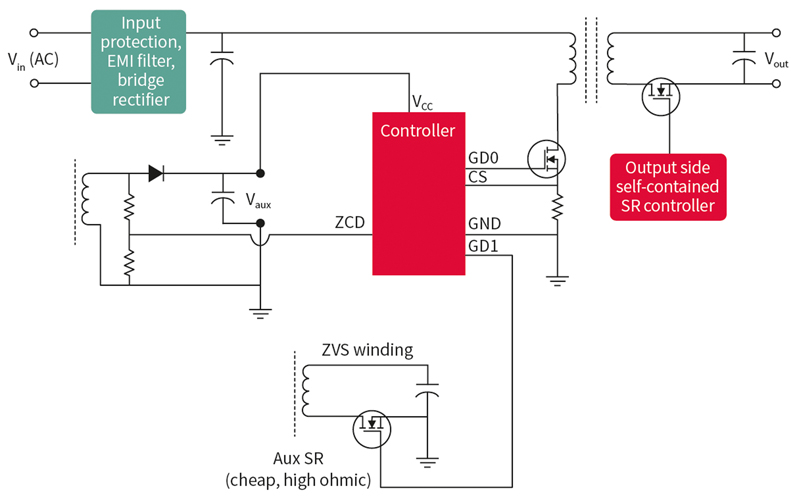
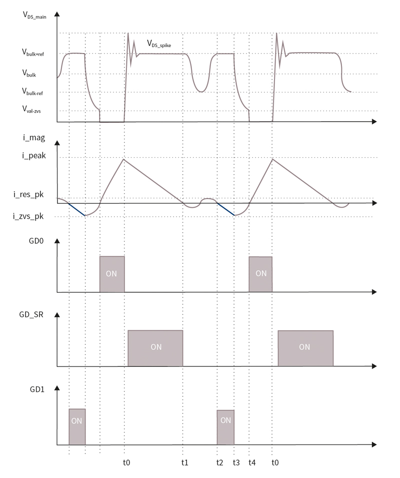
With the intention to optimize flyback performance, Infineon introduced the forced-frequency resonant (FFR) flyback in the industry. This topology has several outstanding performance features including but not limited to zero voltage turn-on, fewer external components, and smaller difference in frequency during high- and low-line input operation. Figure 3 shows the topology and the ZVS operation principles.
After the primary MOSFET is turned off at t0, the synchronous rectification (SR) MOSFET will turn on slightly delayed by a short blanking time. At t1, when the demagnetizing current ideally goes to zero, the SR MOSFET is turned off, and then the magnetizing inductance Lp and Ceqv oscillate. The voltage of the primary MOSFET will oscillate from Vbulk+Vref to Vbulk-Vref. In case the auxiliary MOSFET is turned on at t2, the resonant peak of the primary MOSFET will mean the magnetizing current is zero, so the i_mag value will accumulate to a negative value. During this controlled ZVS on-time, the VDS of the primary MOSFET is clamped to Vbulk+Vref. Once the peak current reaches i_zvs_pk, the auxiliary MOSFET will turn off, and since this current is stored in the magnetizing inductance and in the reverse direction, it will continue to flow in that direction and release the energy stored in Ceqv. This duration in the IC is controlled by a configurable tZVSdead parameter. Therefore, at t4, the drain voltage of the primary MOSFET reaches its minimum and turns on the primary MOSFET greatly reducing turn-on losses, which is almost ZVS. As shown in the figure, energy is proportional to Vbulk, and so is the ZVS on-time.
ZVS pulse insertion is based on nano-DSP core and memory info. The IC recognizes the next switching cycle period and ZVS dead-time and ZVS pulse on-time. Therefore, assuming the IC main gate turn-on time is also fixed, subtracting these two parts (the ZVS dead-time and the ZVS pulse-on time) from the switching period will decide the ZVS pulse starting point. When the CS signal reaches the current command, the main gate off-point can also be determined.
Click image to enlarge
Figure 3a & b: The recommended FFR ZVS topology (a) and the ZVS operation principles (b)
Click image to enlarge
Figure 3a & b: The recommended FFR ZVS topology (a) and the ZVS operation principles (b)
MOSFET packaging considerations for performing density designs
In addition to selecting the fitting topology, choosing the right high-voltage MOSFET is also a key to a high-efficiency design. Infineon’s CoolMOS™ series with their ever increasing performance can help reduce switching losses. By reducing the total gate charge (Qg) of the MOSFET and reducing the energy stored in the output capacitance - which energy needs to be discharged every cycle during hard switching (Eoss ) -, the switching loss of the MOSFET can be improved. By reducing these total charges which are dissipated in every switching cycle, the efficiency of the system at light loads can be improved. The conduction losses of the MOSFET are reduced through the continuous improvement in the CoolMOS™ technology, leading to ever-improving device temperature coefficient too. With these improvements in conduction- and switching losses, new technologies provide the possibility to shift to higher RDS(on) MOSFETs reducing the overall system costs or increasing the overall system switching frequency that reduces size the form factor and the number hence also the costs of passive components.
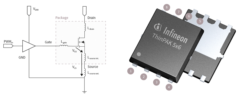
In charger designs, the total loop inductance of the MOSFET (consisting of the gate-source and drain-source inductances) is important to prevent the MOSFET turning on again and also to reduce EMI. Compared with the DPAK or the FullPAK THD packages, ThinPAK offers a reduction in gate-, drain- and source inductances (shown in Figure 4). Compared with the DPAK package, the internal source inductance of the ThinPAK is also reduced, by 63 percent.
To reduce the ringing on the gate of the MOSFET, the total gate source inductance (Lgate_loop = Lsource + Lgate) is important. When the LC resonant tank formed by the gate capacitance (Ciss) and the total gate loop inductance (Lsource ext. + Lgate_loop) is excited by a square wave driving waveform, this can cause ringing on the gate of the MOSFET. By reducing the total Lgate_loop , the amount of ringing seen on the gate of the MOSFET can be reduced.
Click image to enlarge
Figure 4 The ThinPAK package enables reduction of the parasitic inductance in the gate drive loop
In a nutshell
With the high-performance digital ZVS controller XDPS21081, this 65W reference design achieves up to 93 percent efficiency by implementing QR during low-line voltage input and FFR during high-line voltage input. When the controller is used together with CoolMOS™ superjunction MOSFETs in ThinPAK, the charger can be placed in a compact case. In addition, the simple EMI filter design and low BOM cost can help design engineers improve charger design capabilities.
Discover our reference designs, boards and design support documents at www.infineon.com/usb-pd!