Well-designed I/O interfaces greatly lower thermal generation in PLC digital I/O modules
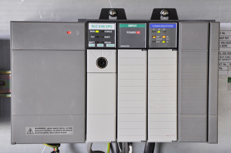
Automated factories employ sensors and I/O modules to control their industrial processes. As they increase in sophistication and shrink in size, they are enabling the fourth industrial revolution, dubbed Industry 4.0. A single module (see Figure 1) can have up to 64 channels, and a typical factory floor may utilize several modules. With the number of channels skyrocketing easily into the thousands and the size of the module enclosures constantly shrinking, it is understandable that the power dissipation and heat generation of each channel is a primary concern. Let’s look at a common solution for handling power, then present one that greatly improves the power savings at the critical interface point between the module and the external environment.
Click image to enlarge
Fig 1. Digital I/O Module System
The Digital I/O Module System
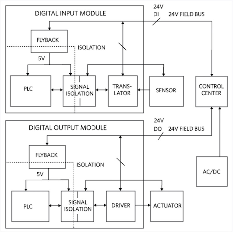
Figure 2 illustrates a typical digital I/O module system block diagram. A central hub (Control Center) takes the AC line power and converts it to 24V DC which is delivered to the I/O modules, along with the corresponding digital input (DI) and digital output (DO) data. The factory environment is rugged – due in part to electric and magnetic interferences and over-voltages. The sensitive electronics of the controller must therefore be protected. Accordingly, each module’s programmable logic controller (PLC) is powered via an isolated step-down voltage regulator (“Flyback” in Figure 2).
Click image to enlarge
Fig 2. Digital I/O Module Block Diagram
At the digital input module (DIM) a rugged voltage level translator interface powers the sensor, receives its information, and passes it along to the PLC via a digital isolator or opto-coupler. A similar power, signal and isolation chain on the digital output module (DOM) leads to the on board driver, interfacing to the external actuator. The DIM’s input translator and the DOM’s output driver are the primary locations where power is transferred, consumed and dissipated as heat. With modules becoming smaller, no longer leaving space for cooling fans, the traditional, inefficient solutions fall short. New, highly efficient solutions are needed.
DIM Translator Discrete Implementation
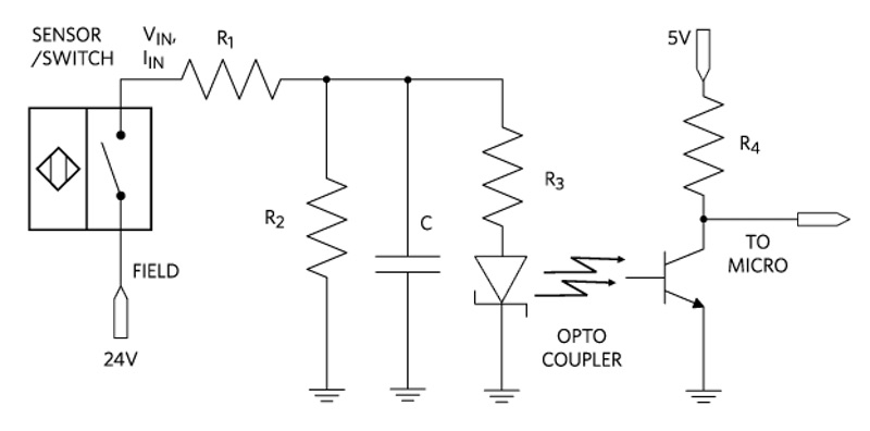
A common way to interface the digital input module is illustrated in Figure 3. The high voltage rail (24V) is filtered and divided down (via R1, R2, R3 and C) into the anode of a photodiode, part of the optocouper performing the signal and power isolation path. This solution is costly and bulky, as it requires an optocoupler for each sensor chain.
Click image to enlarge
Fig 3. Discrete Translator
As far as power consumption, the worse-case scenario is that in which a poorly regulated 24V swings up to 30V. Assuming that the input channel is designed for a trip point at VTRIP=VIN=9V and ITRIP=ILIM=2.4mA (which meets IEC61131-2 type 1 switch requirements), we can derive the maximum power dissipation per channel (neglecting the photodiode, Vbe, for simplicity):
RIN = R1 + R2 || R3 = 9V / 2.4mA = 3.6KΩ
IINMAX = 30V / 3.6KΩ = 8.3mA
PMAX = 30V X 8.3mA = 250 mW per channel
For a card with 16 digital inputs this adds up to a whopping 4 watts of power dissipation. The corresponding heat generated in the small module enclosure can raise the temperature to unacceptable levels.
DIM Integrated Interface Solution: Current Limit
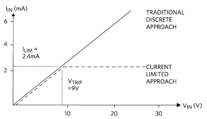
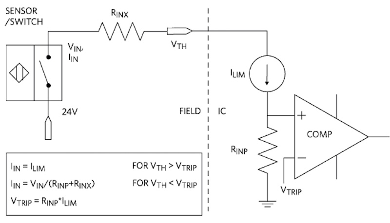
A clever way to limit the translator power losses is to clip the resistor curve as shown in Figure 4. In principle this is done by placing a current source ILIM in series with the resistors (RINP , RINx in Figure 5), such that ILIM kicks in at the set knee voltage, VTRIP (VTRIP=RINP*ILIM). ILIM saturates (VCESAT ≈ 0) at VTH<VTRIP. The equations shown in Figure 5 describe the behavior of the circuit for the current limited approach (dashed line) in Figure 4.
Click image to enlarge
Fig 4. Current Limited Approach
Click image to enlarge
Fig 5. Current limited Integrated Translator
With this technique we can limit the worst case power dissipation to:
PMAX = 30V X 2.4mA = 72 mW per channel
This corresponds to a reduction of the power dissipation by 3.5 times or 71% compared to the traditional approach. Correspondently, a 16-channel card will consume only about 1.1 Watt. The system will be able to run much cooler, resulting in higher reliability and lower operational costs.
For example, the MAX31910, MAX31911, MAX31912, MAX31913 MAX31914 and MAX31915 family of Octal, Digital Input Translators/Serializers translate, condition, and serialize the 24V digital output of industrial sensors down to 5V CMOS-compatible signals required by microcontrollers. They achieve an outstanding low-power dissipation of 72mW by implementing this current limiting solution.
DIM Integrated Interface Solution: Switched Current Limit
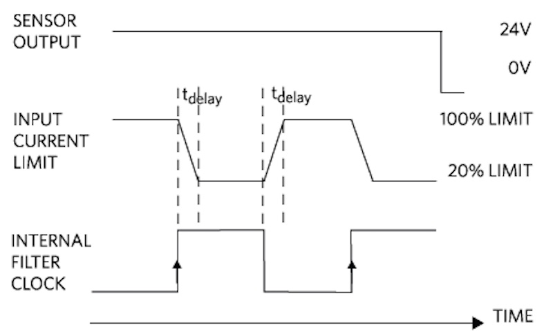
A further improvement can be introduced using a technique patented by Maxim Integrated, known as “Switched Input Current Limiting”. This technique is implemented in the MAX31910, MAX31912, and MAX31914 ICs. The input current, in addition to being limited, is duty cycled. The comparator output is latched on the rising edge of the clock, and the current limit amplitude is immediately reduced down to 20% of the initial value, for a time equal to 50% of the internal digital filter clock period (see Figure 6).
Click image to enlarge
Fig 6. Switched, Current Limited Translator
The new power dissipation is:
Pmax ≈ 0.6(Vmax x Imax ) = 0.6(30V x 2.4mA) ≈ 42 mW per channel
This corresponds to a reduction in power dissipation of 6 times or 83% compared to the traditional approach. A 16-channel card in this case will consume only 0.67W.
DOM Power Saving Solution
There is room for power savings in the Digital Output Module as well. The actuator could be, for example, a motor requiring 12 Watts of power at 500mA (24V typical input, 30V max). This power is applied through a MOSFET switch which will dissipate power in proportion to its RDSON.
A typical integrated circuit driver with a maximum RDSON of 320mΩ over temperature and a quiescent current of 12mA per 8 channels will dissipate:
PDISS(RDSON) = 320mΩ * (500mA) 2 = 80mW per channel
PQUIESCENT = 12mA * 30V = 360mW per 8 channels at 30V maximum input voltage
For a card with 16 digital outputs this adds up to 2 watts of total power dissipation.
The MAX14900E Octal, High Speed, Industrial, High-side Switch, an RDSON of 162mΩ (max) over temperature and quiescent current of 3mA (max) for 8 channels, leading to a fraction of that power dissipation:
PDISS(RDSON) = 165mΩ * (500mA) 2 = 41mW per channel
PQUIESCENT = 3mA * 30V = 90mW per 8 channels
For a card with 16 digital outputs this adds up to a miserly 0.836 Watts of total power dissipation vs the previous 2 Watts; a reduction in power dissipation of 58%.
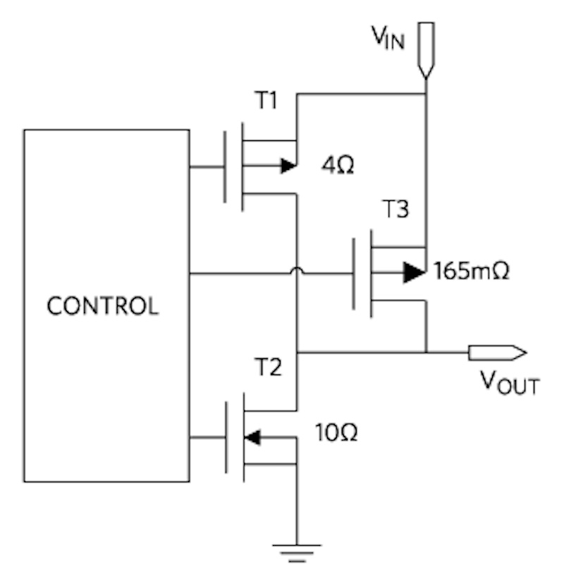
Figure 7 illustrates a single channel output stage of the MAX14900E. In addition to a 165mΩ high-side power MOSFET, each output has a push-pull stage.
Click image to enlarge
Fig 7. MAX14900E Single Channel Output Stage
When configured in high-side mode, each driver can safely source 850mA (max) load current continuously. The high-side switches have active current limiting in the range between 1.4A (min) and 2.0A (max). When a driver is in push-pull mode, the output drives resistive/capacitive loads at high switching rates with load currents up to 100mA to ground.
The importance of power saving
We have reviewed, at a high level, an industrial sensor system, from the sensor to the actuator. We highlighted the architectures of the digital input and digital output modules, and discussed the importance of power savings, especially where the modules interface with the real world.
Next, we examined the digital input module and showed how Maxim’s integrated current limited and duty-cycled approach drastically reduces the module’s power dissipation compared to the traditional discrete approach. Finally, we discussed the digital output module and how Maxim Integrated’s output driver with best-in-class RDSON drastically reduces the power dissipation compared to a common integrated solution.