Efficient WBG Power for Medium Voltage Applications
In high voltage applications, such as locomotive traction drives and medium-voltage industrial drives, wide bandgap semiconductors offer numerous advantages….
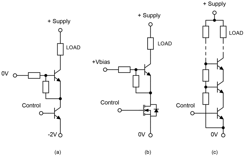
Figure 1: Example historical cascode circuits
Perhaps the power conversion industry is now familiar with the concept of the ‘cascode’ device when applied to silicon and wide band-gap semiconductor hybrids, achieving a close approximation to the normally-off, ideal switch, with easy gate drive and a range of other benefits. The idea goes back to 1939 when Hunt and Hickman proposed the idea of cascaded vacuum tube triodes or ‘cascodes’ for voltage stabilisers. Cascodes subsequently found use in amplifiers, as they were found to be less noisy and easier to bias than the pentode tubes of the time.
In the era of semiconductors, cascodes have reappeared in various guises as amplifiers and switches, with combinations of bipolar transistors and MOSFETs, sometimes called ‘emitter switching’ circuits, for example Figures 1a and 1b. A particular advantage of the cascode is the ability to control a high-voltage transistor with another low voltage type, for example as in Figure 1b, where a low-cost, high-voltage bipolar transistor is controlled by a low-voltage, easy to drive MOSFET. A natural extension of this idea is to add further devices to increase the operating voltage level up to the kV level, for example as in Figure 1c where the high voltage stress is divided across the upper transistors. The idea is sound, but with bipolar transistors, base currents represent significant loss in the biasing resistors, and in switching applications, the base drive is too simplistic giving slow switching speeds. Bipolar implementations are also unable to conduct in the ‘third quadrant’, passing current up from ground into the load as is needed in ‘commutating’ and hard-switching applications, requiring an extra parallel diode.
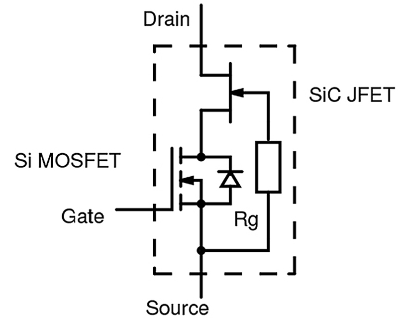
A modern cascode – the SiC FET
Today, the ‘gold standard’ of the cascode is the SiC FET (Figure 2), a combination of a low voltage silicon MOSFET and high voltage silicon carbide normally-on JFET. The SiC FET gives nanosecond switching times, a fast and low recovery charge body-diode effect for third quadrant conduction, very low gate charge and low switching energy loss. On-resistance is best-in-class for a given die area compared with IGBTs, Si MOSFETs, SiC MOSFETs and GaN HEMTs. The well-publicized advantages of SiC as a wide band-gap material are retained – high voltage and high temperature operation but with the easy gate drive of a low voltage Si-MOSFET. The SiC FET is also rugged with more than enough avalanche and short-circuit capability for use with modern circuit protection schemes.
Click image to enlarge
Figure 2: The modern cascode with Si-MOSFET and wide band-gap SiC JFET
In the ‘SiC FET’ cascode implementation of Figure 2, when the Si-MOSFET is turned on via its gate, the JFET source and gate are effectively shorted and the JFET conducts. Current passes through the JFET and MOSFET drain-source channels with the conduction loss fixed by the JFET, as the low-voltage Si-MOSFET on-resistance is extremely low compared with that of the high-voltage SiC JFET. When the Si-MOSFET is off, the JFET source voltage rises to the point where its gate-source threshold of a few volts negative is exceeded and the JFET turns off. Because of the ratio of device capacitances, dynamically, the voltage across the Si-MOSFET remains low.
Switching higher voltages
When switching voltages over about 600V, IGBTs are often considered as a low-cost and proven solution but the devices have always suffered from slow switching speeds and ‘tail current’ losses on switch-off. Modern applications are increasingly requiring faster switching to extract system advantages in size and cost, and Si or SiC MOSFETs seem to be an obvious alternative. However, high voltage MOSFETs are relatively more expensive and exhibit high on-resistance. When several kV needs to be switched, MOSFETs become very specialized and the thick epitaxial layer necessary for the high voltage rating increases on-resistance, with applications typically requiring paralleled devices to achieve acceptable conduction loss. Device input and output capacitance are also all paralleled, slowing switching, increasing losses and requiring more gate drive power. At high voltage, bridge converter circuits require isolated ‘high-side’ drives and because of the high dV/dt experienced, the driver and its power supply must have very low barrier capacitance which becomes more challenging to achieve at higher gate drive power levels.
Another consideration is that high voltage SiC-MOSFETs have excessive stored charge when their body diode conducts (Qrr), especially at high temperature, necessitating use of a parallel JBS diodes which are costly, take up space and ultimately can limit the current rating of high-voltage power modules.
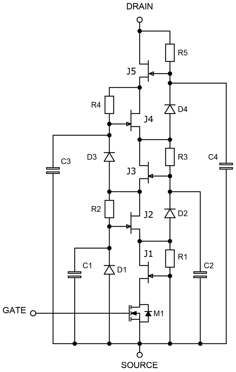
Supercascodes can be an ideal solution
One solution to the problem is to revisit the technique of series connection of devices in an example ‘supercascode’ arrangement of the SiC FET as shown in Figure 3.
Click image to enlarge
Figure 3: The SiC FET ‘Supercascode’ topology
In the topology, the single SiC JFET is replaced by multiple devices in series and biased so that as J1 switches off under control of the Si-MOSFET, M1, the remaining JFETs turn off simultaneously with the drain-source voltages sharing equally. In this arrangement, off-the-shelf, lower voltage SiC JFETs can be used, with ratings typically available up to 1700V each. The low voltage Si-MOSFET does not change, so its gate drive remains easy and JFET device capacitances are now in series rather than parallel. The diodes in the circuit are used to clamp the blocking voltages of the JFETs, the resistors provide the desired bias current for the diodes during the off-state and the capacitors ensure that the JFET voltages are dynamically balanced and that the JFET turn-on and turn-off processes are synchronized.
The fast body diode effect of the SiC FET is retained so parallel diodes are not needed for third quadrant operation and the supercascode retains the robust short circuit and avalanche capability of the cascode structure.
There are additional benefits with the supercascode; over-current and short circuit sensing is much easier as current in just the Si-MOSFET can be monitored. The Si-MOSFET can be fabricated with isolated cells to show typically a 1:1000 current sense signal, which in a cascode, does not suffer from inaccuracy due to self-biasing. De-saturation detection is also easier as the drain of the MOSFET can be monitored, which never exceeds a few volts, allowing a low-voltage Schottky diode to be used in the standard detection circuit.
Overall, component cost is lower than with paralleled high-voltage MOSFETs, switching speed is far better than with IGBTs, functionality is increased and using standard commercially available parts, design risk and development time are substantially reduced.
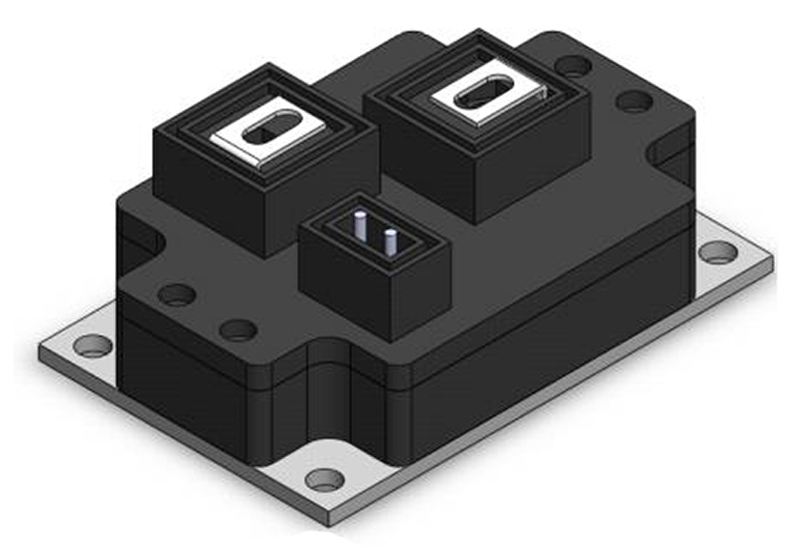
Practical results
Since 1999, UnitedSiC has developed a wide range of SiC FET cascode parts, in a now well-established process and with automotive quality approvals proving product reliability. They have also pioneered the supercascode concept. One demonstration device in a custom package rated at 4.5kV/40A integrates the components of Figure 3 with five, 1200V/14 milliohm JFET die and a 20V/5 milliohm Si MOSFET (Figure 4).
Click image to enlarge
Figure 4: 4.5kV, 40A supercascode prototype from UnitedSiC
Measured turn-on speed for the device is 105ns with EON 12.7mJ and turn off is 56ns with EOFF 1.4mJ for a total switching energy ETOT of 14.1mJ. This could be compared with an IGBT of similar rating which shows ETOT as 305mJ. Reverse recovery charge QRR for the supercascode at 2.3kV/25A is also impressively low at just 1.61µC at a di/dt of 1290A/µs, similar to that of a single SiC Schottky diode.
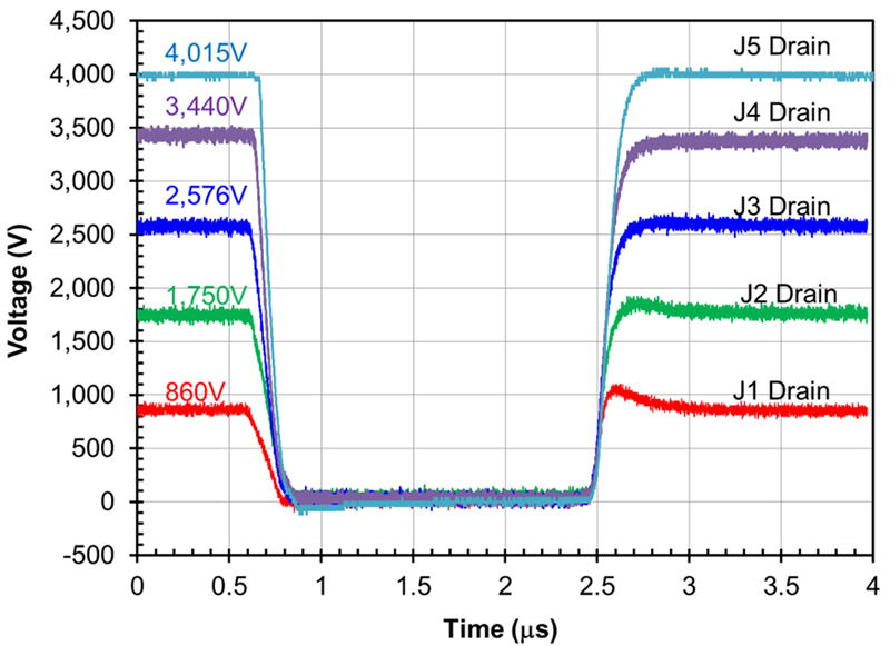
Crucial to performance and reliability is the dynamic balancing of the series SiC JFET voltages.
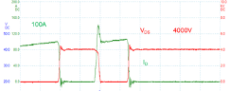
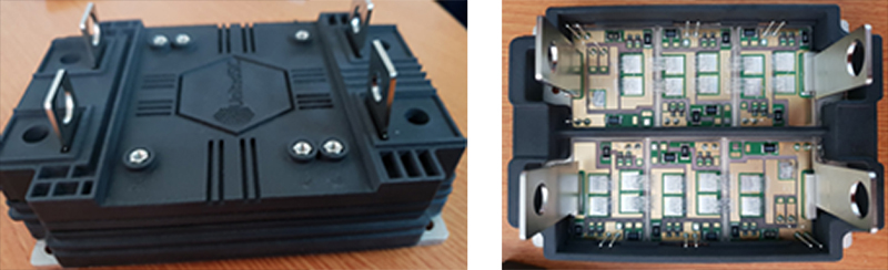
Extending the work further, UnitedSiC has also demonstrated a 6.5kV/100A half-bridge supercascode module (Figure 5) which shows ETOT values of 69mJ and a QRR figure of 3.7µC, both more than an order of magnitude better than an IGBT of similar headline ratings. The module is a good fit for the applications of solid-state transformers, wind, traction and HVDC. Another prime application would be future 350-400kW EV fast chargers with a medium-voltage 4160VAC three-phase supply, with the 6.5kV/200A used in a three-level inverter.
Click image to enlarge
Figure 5a & 5b: A supercascode half-bridge module rated at 6.5kV, 100A
Click image to enlarge
Figure 6: 6.5kV Supercascode prototype shows excellent dynamic voltage balancing
The concept is scalable to even higher voltages with UnitedSiC achieving a module with 40kV/1A rating by stacking supercascode blocks, utilizing a total of 30 standard JFET die, each 1700V rated. The stack measured at 18 ohms on-resistance with just 75µA leakage with 30kV applied.
Conclusion
The SiC FET has proven its credentials as a step closer to the ideal switch and now its advantages can be realised at tens of kV rating with the ‘Supercascode’. Built up from series connections of standard off-the-shelf die with supporting passive components, all integrated into industry standard or custom packages, the supercascode is a high-performance, cost effective and low risk solution to high-voltage switching for existing and next-generation applications.