eGaN FETs improve performance in industrial POL converters
Converter choice impacts cost-effectiveness and efficiency
Designers of point of load (POL) converters used in 24 VDC systems traditionally have had to decide between the high cost of an isolated converter and the low frequency and efficiency of a buck converter. When compared with the 12 V POL converter common in computing systems, the higher voltage of the 24 V POL converter increases FET voltage to at least 40 volts to accommodate switch-node ringing and increases commutation and COSS losses. eGaN FETs, such as those from EPC, offer ultra-low QGD for low commutation losses and low QOSS for lower losses when charging and discharging the output capacitance. In addition, the innovative Land Grid Array (LGA), wafer level packaging of EPC's eGaN FETs allow ultralow inductance in both the high frequency power loop and gate drive loop, and most importantly, the path common to these loops, known as the common source inductance (CSI) to help minimize current commutation losses. Low charge and CSI of eGaN FETs allow designers to push power density higher by pushing frequency higher without the efficiency penalty of traditional MOSFETs. Experimental Setup The circuit that will be discussed is a buck converter with 24 VIN, 1.2 VOUT with an output filter inductance of 300 nH, switching at 1 MHz, and an output current of up to 20 A. The eGaN FET boards were run with 5 V gate drives using the LM5113 eGaN FET driver from Texas Instruments. As MOSFETs run more efficiently with a higher gate voltage, 8 V, ISL2111 is used to reduce RDS(ON) and limit gate drive losses. Layouts for MOSFET and eGaN FET boards were made as similar as possible to minimize board parasitic differences. There are two key areas where inductance is critical to performance, the CSI (LS) and the inductance of the high frequency power loop LLOOP. CSI external to the package was minimized in all designs by separating the gate drive loop from the power loop right at the source foot on the PCB for each package. Additionally, a second eGaN FET board was designed to take advantage of the eGaN FET's small size and interleaved drain and source terminations which allows a very low inductance PCB layout. Common figures of merit (FOMs) used to compare FETs are RDS(ON) x (QGD + QGS2) and RDS(ON) x (QOSS + QRR) where QGS2 is the portion of QGS where current is commutated [1]. FOMs are good for comparing technologies, but within a technology, scaling the die size trades switching losses against conduction losses. For low duty cycle buck applications, the low capacitance of a small device far outweighs its high RDS(ON) for the control switch, but the opposite is true for the rectifier switch. For each socket and a given set of operating conditions, efficiency rises, peaks at an optimum die size, then falls as die size increases. The Infineon BSZ097N04LSG was used for the MOSFET control switch and BSZ040N04LSG was used for the rectifier switch. For the eGaN FET boards, the EPC2015 was used for both control and rectifier switches. It should be noted that with the EPC2015 as the eGaN FET control switch, switching losses grossly outweigh on-state losses, and there is much room for efficiency gains from future die optimization. The first layout is a vertical layout where the FETs were on one side of the board and input capacitors on the other. A side view of the vertical layout is shown in figure 1a, and the comparison of the MOSFET and eGaN FET layout is shown in figures 1b and 1c. The significant layout advantage of the eGaN FET board was a smaller high frequency loop that was made possible by the smaller size of the eGaN FET and the lower package parasitics of the LGA package. The high frequency loop inductance for the eGaN FET board is estimated at 1.0 nH while the MOSFET board was estimated at 2.0 nH. It should be noted that the bulk of the high frequency loop inductance in the MOSFET design is the package inductance. In most cases, MOSFET manufacturers do not specify package inductance.

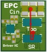
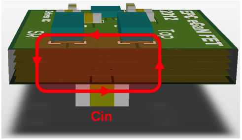
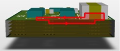
With much of the parasitic inductance being in the board, and the interleaved source and drain of the LGA package, eGaN FETs are able to take advantage of further layout optimization. A second eGaN FET layout has input capacitors placed next to the control FET with the return from the rectifier FET being brought back on the second layer for flux cancellation, reducing the high frequency DC loop inductance. Between the two eGaN FETs and below the rectifier FET are interleaved vias of switch-node and power return that match the lands of the rectifier switch. The rectifier source vias between the two FETs reduce the length of the high frequency power loop, lowering inductance. The rectifier source vias below the rectifier FET reduce resistance, thus conduction losses during freewheeling. Interleaving the power return and switch-node vias provides opposite current flow in them reducing AC conduction losses by reducing eddy and proximity effects [3]. High frequency power loop inductance is estimated to be 400 pH. This optimal layout is shown in figure 2.
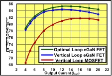
Results Efficiency results are shown in figure 4 for the vertical layouts of the MOSFET and eGaN FET circuits along with the optimized eGaN FET circuit. The efficiencies of both eGaN FET boards completely envelope the efficiency of the MOSFET board. 20 A efficiency was increased by 2% while 4 A efficiency was increased by over 9.5%.
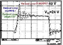
High frequency power loop inductance had a dramatic effect on switch-node overshoot and ringing. The optimal layout eGaN FET board peaked just above 24 V and rang out in 10 ns, while the MOSFET board peaked over 40 V, and took half the on-state pulse time to ring out as shown in figure 3b.