Enabling More Effective Battery Charging Over USB Interconnects
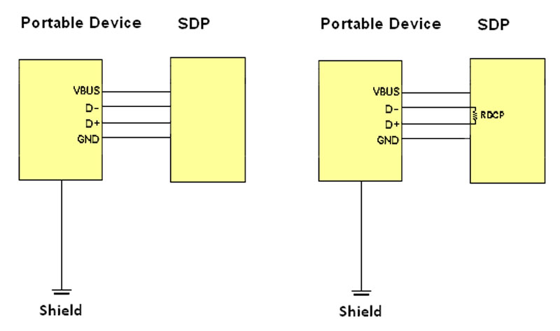
Figure 1: Difference between a DCP and SDP
Developed in the mid 1990s, USB has gone on to become the most widely used data interface on the planet. Its huge popularity has certain additional upshots which are also now being realised. Market pressures are beginning to make it attractive as the principal way to power electronics hardware. As of January 2011, the European Commission (EC) introduced a policy that means all smartphone/data-enabled phone handsets sold in Europe need to have the ability to be charged via a standard micro USB connector. This will help consumers to escape from the irritation of having to rely on various proprietary cables to charge each individual portable electronics item they possess. USB offers the means with which to charge multiple portable devices through a single �universal' power source, resulting in far greater convenience. There are challenges with its employment in this role, however. Previously the charging capability of USB was fairly limited. The amount of current available from a standard USB Host port was really only suited to powering computer peripherals, such as keyboards, mice and card readers. USB 2.0 supports a charging current of up to 500 mA, which can translate into a prolonged charging process for some batteries. At the same time, the public at large is requiring shorter recharge periods. In this environment, the USB Charging Specification Version 1.2, was announced in early 2011, offering new powering modes that increase flexibility when it comes to replenishing devices' batteries. The document introduces the concept of a Dedicated Charging Port (DCP) which enables a maximum current of 1.8 A to be supported. This nearly quadruples the current that a Standard Downstream Port (SDP) USB 2.0 connection can carry, resulting in considerably quicker charge up time. All about the DCP The USB interface is made up of four shielded wires. These are: • VBUS which is used to power the connected peripheral • D- which is the negative data terminal • D+ which is the positive data terminal • GND which is the ground connection In a DCP, both the D+ and the D- ports are shorted together with a 200 Ohm resistor, so that data transfer is prevented. It indicates to the connected peripheral that the port is fully focussed on the charging function and does not provide Host functionality. It is vital that any portable device that is to be connected with a USB port can differentiate between it being a DCP or an SDP. This will allow it to take advantage of the larger charging current that is available.
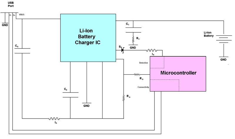
DCP Identification Figure 2 shows an example of a charging circuit in line with version 1.2 of the USB charging specification. It includes a large number of discrete components and requires the systems' microcontroller to take care of the identification procedure. This means that a proportion of microcontroller's valuable processing capacity cannot be devoted to the core application, thereby impinging on the system's overall performance. Furthermore, a relatively large bill of materials is called for, as well as many hours to write the necessary code and to implement the circuit design in a way that makes it fully effective.
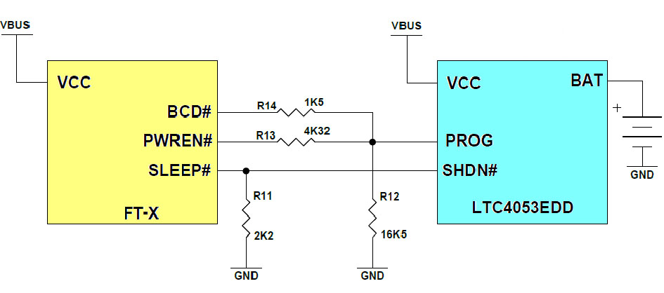
FTDI has endeavoured to simplify USB charging, so that development time, system complexity and utilisation of engineering resource are all minimised for the greatest return on investment. To this end it has introduced the X-CHIP series of USB controller ICs, which has a feature set that supports the new concepts of USB battery charging. Circuitry inside each IC enables the portable device it has been incorporated into to detect when it becomes connected to a DCP. Once a DCP is detected, the X-CHIP asserts a signal on one of its CBUS pins to enable charging to begin. Figure 3 describes a battery charging application based around the X-CHIP. The circuit will charge a battery when connected to either a USB Host port or a DCP. The CBUS pins can be used to control the charging rate of the battery depending on the power source which has been detected and its associated current limit. The charge rate of the battery is defined by the resistance connected to the PROG pin of a Linear Technology LTC4053 battery charging controller. The CBUS pins are: • The BCD# is an open-drain active-low output signal. It is asserted to indicate when the X-CHIP has been connected to a DCP. • The PWREN# is open-drain active-low output signal. It indicates that the X-CHIP has been enumerated by the USB Host controller. It is used to select the resistance value on the PROG pin in order to enable 500 mA charging. • The SLEEP# is a push-pull active-low output signal. It indicates when the X-CHIP has been put into USB suspend mode. It is used to shut down the LTC4053 when the device is powered from a USB Host and the Host has put the X-CHIP into suspend mode. In Figure 3, the resistance of the PROG pin of the LTC4053 is set by resistors R12, R13 and R14. The BCD# is used to configure the resistor network on the PROG pin to set approximately 1 A charging current. The BCD#, PWREN# and SLEEP# outputs have been designed to minimise the external circuitry required for charging applications. Normally external MOSFET devices are required to select the range. As already mentioned, the X-CHIP asserts its BCD# signal to indicate the detection of the DCP. This open-drain output short circuits R14 to ground and the PROG pin of the LTC4053 will therefore have a resistance of 16.5 k? in parallel with 1.5 k? to ground. This results in a charging current of approximately 1 A being initiated. When the X-CHIP is connected to a standard USB Host controller, this pin is not asserted and the device operates as a traditional USB interface chip. Since the BCD# signal is open-drain without an internal pull-up, it can be used to pull resistor R14 to ground without the need for utilising any external MOSFETs. During start-up of the device, the CBUS pins will default to an input with weak pull-up until the MTP ROM is read. This will occur for approximately 14 ms and the CBUS pins will then take their selected function and behave as described elsewhere in this article. Conclusion Thanks to their widespread use, USB ports are clearly a convenient place for portable devices to draw power from, potentially delivering as much as 10 W to a variety of different devices through a single interconnect. Furthermore, the push to standardise on USB charging by various countries (including China and EU member states) is allowing consumers to employ fewer charging cables. This will increase convenience while reducing the quantity of electronic waste entering the environment each year (which was being caused by customised adapters). Lastly, by using an integrated approach rather than relying on discretes it is possible to create far more optimised charging circuits in terms of space, components and engineering resource. In the end, USB is not only the most popular wired, digital interconnect, but a key system element for providing power and charging the batteries of electronic products. www.ftdichip.com


