A new interconnect approach promises to deliver precise, accurate voltages at high power levels to semiconductor devices under test.
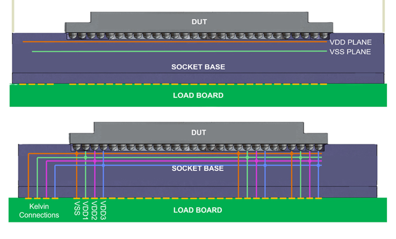
Figure 1: With tester voltage references VSS Sense and VDD Sense on the tester side of the socket, parasitic losses can decrease voltage control
The arrival of high-performance computing (HPC) and artificial intelligence (AI) is having significant effects on the semiconductor devices developed to serve these applications. AI and HPC chips do have some differences. AI chips are optimized for deep learning and neural-network processing and can tolerate relatively low precision—16-bit floating-point, for example. In contrast, HPC chips feature many-core architectures with high precision—64-bit floating point, for example. They do have some functional similarities, however—GPUs, for example, find use in both applications. But one feature they definitely have in common is an appetite for ever-increasing amounts of power, which is exacerbated by fab process shrinks.
Because of these growing power requirements, the status quo has major shortcomings when it comes to delivering power to AI and HPC devices under test (DUTs). Fortunately, Advantest is developing a new interconnect design approach to mitigate these shortcomings.
Power challenges
The power and heat-dissipation trends combined with fab process shrinks present three challenges, two of which are interrelated. First, some logic circuits on a chip may have high workloads for short periods of time, and as a result, the DUT experiences areas of very high localized concentrated current draw instead of seeing currents evenly spread out over the entire array of the device’s solder balls. The locally concentrated current draw leads to the second challenge—areas of locally concentrated heat dissipation, resulting in hot spots. Aggravating the situation is that the silicon itself, whose processing operations require additional intermittent currents, adds to the local heating problem.
The third challenge is maintaining voltage stability and power integrity not only at high current levels but also at high di/dt rates as the workload varies with time across the device. These challenges will become increasingly difficult to address as power increases, and current industry trends suggest that power consumption will exceed 3 kW per device in 2027. Yet, as power and current increase, devices are requiring even tighter voltage control.
Load board vs. socket
Thus far, the drive for power integrity in the semiconductor test environment has rested with the load-board manufacturer. Customers clamor for better power integrity, so the load-board vendor adds more power layers and more capacitors and optimizes routing. But efforts in this regard are delivering diminishing returns. The load-board vendors might push back and suggest more of a focus on the test socket, but the socket has thus far not seemed a viable target for improvement.
Figure 1 shows the limits of today’s standard interconnects. If the tester voltage reference resides on the load-board side of the interconnect, parasitic losses in the socket pins decrease control and sense accuracy. Repurposing some VDD and VSS pins for sensing, as shown in the figure, can help, but with current levels increasing, there is rarely sufficient margin to allow for such repurposing.
The socket solution
Advantest, which makes both load boards and sockets, has investigated ways to improve voltage sensing and control and has developed an alternative to the standard interconnect approach of Figure 1. The company has integrated the VDD and VSS planes as conductive layers within the test socket, as shown in Figure 2 (top), placing them closer to the DUT. This approach can be extended to add multiple voltage rails to enable the test of DUTs with multiple voltage domains, as shown in Figure 2 (bottom). With this approach, planes and traces can connect additional VDD and VSS pins to establish Kelvin connections outside of the DUT footprint, a location where it is more likely there will be room for additional pads that can be brought back to the tester.
Click image to enlarge
Figure 2: With VDD and VSS planes integrated into the test socket (top), Kelvin connections can be placed outside the DUT footprint (bottom)
It should be noted that increasing bandwidths and Nyquist frequencies necessitate the use of coaxial structures with conductive shielding around signal pins, which must be integrated into the socket to meet near-end crosstalk (NEXT) and far-end crosstalk (FEXT) requirements. In addition, impedance tolerance tightens, so impedance must be well controlled.
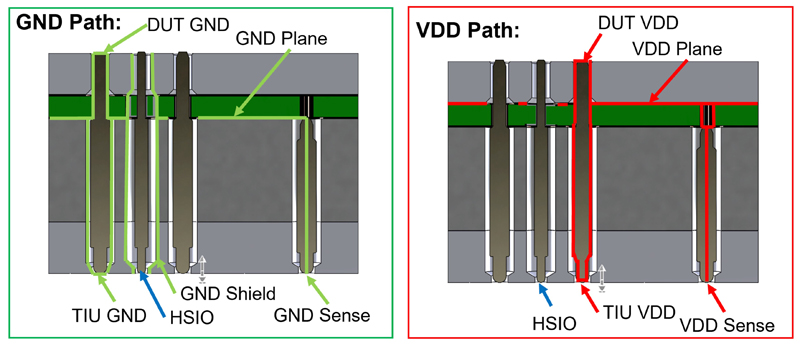
Figure 3 shows the socket design details, with the ground path and ground plane on the left and the VDD path and VDD plane on the right. The figure also shows both DUT and test interface unit (TIU) ground and VDD connections and the corresponding sense connections, as well as high-speed I/O (HSIO) connections. Note on the left the ground connection to the metal body around the HSIO pin, which extends to the metal layer on top, because it is critical to have a full-height shield from the bottom to the top of the pin. On both the left and the right, the sense pins connect to the load board outside of the DUT footprint.
Click image to enlarge
Figure 3: The ground path is highlighted in green (left), while the VDD path is highlighted in red (right) in this patent-pending design
Several additional considerations apply to using the socket to improve power integrity. The socket’s VDD and VSS planes add capacitance near the DUT, and additional capacitors may be added, with interstitial capacitance a possibility to filter out voltage ripple.
Thermal challenges
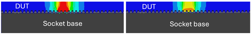
Standard interconnects also present thermal challenges. Interconnect contact elements, such as spring probes, are typically isolated not only electrically but also thermally. They offer poor thermal conduction to the load board and are unable to spread current and heat laterally to mitigate hot spots.
However, locating the VDD and VSS planes in the socket can help with current and heat spreading as well as accurate voltage sensing and control. The planes are most likely copper, which is both thermally and electrically conductive, allowing supply and ground currents to spread across the VDD and VSS planes, boosting the socket’s ability to act as a heat sink and helping to dissipate hot spots. The temperature contour plot comparisons of Figure 4 help illustrate this heat spreading. On the left, with no VDD and VSS planes, a significant hot spot appears. On the right, with the VDD and VSS planes, the hot spot has dissipated.
Click image to enlarge
Figure 4: Standard interconnects tend to be thermally isolated and can lead to hot spots (left), but integrated VDD and VSS planes can reduce hot spots (right)
A question arises as to why not simply use elastomer interconnects—elastomers generally have low inductance and contact resistance, minimizing parasitic losses. However, they are not good conductors of heat, and with elastomers, the current cannot spread laterally. In addition, combining de-coupling capacitors with elastomer interconnects can be difficult, and voltage measurement and control can be compromised. Finally, with elastomers rather than coaxial structures, crosstalk can limit bandwidth, especially with large-pitch devices.
Conclusion
With the arrival of semiconductor devices optimized for HPC and AI applications, rapidly increasing power delivery requirements are presenting significant challenges. Many load-board designs have been nearly fully optimized from a power integrity standpoint, so attention has turned to the test socket. Constructing a socket with integrated VDD and VSS planes and other circuitry can mitigate several of the challenges: it enables voltage sensing close to the DUT without sacrificing pins, it can maintain coaxial shielding along the full length of the interconnect, it can spread current and heat away from localized hot spots, and embedded capacitance can be added to further mitigate transients. Advantest is currently perfecting this approach and is looking for a partner to build and evaluate a solution for its AI and HPC devices.