Author:
Michael Maurer, ROHM Semiconductor
Date
01/28/2021
 PDF
PDF
Click image to enlarge
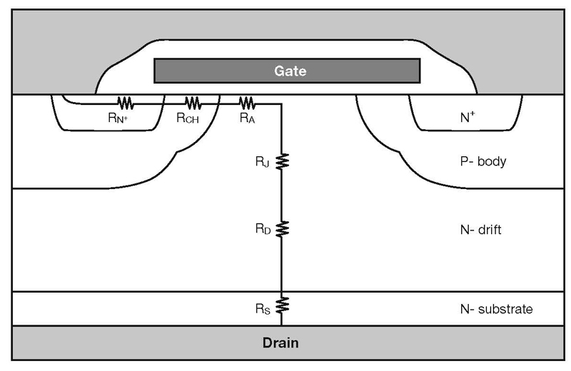
Figure 1: RON is a product of the cumulative resistances from the drain to the source of a MOSFET device
The latest ICs sport faster processors, denser memories/storage, and a wealth of features while increasing reliability and proving lower power usage. Moving to lower processor nodes and relying on lower operating voltages enable these enhancements without dramatically increasing die area, cost, and the need for specialized processes and materials. Conversely, power systems using higher voltages (48V and up) reduce current consumption and ultimately improve power transfer efficiency. In the case of automotive, industrial (robotics), and data communications systems, this results in a growing voltage difference between power systems and applications in the sensor, processor, storage, and communications fields. Bridging this voltage divide has typically required multiple converter stages and trade-offs involving higher ON Resistance (RON = conduction losses), which translates to reduced efficiency. Fortunately, advances in converter technology and packaging have been developed to enhance converter efficiency and reduce conduction losses.
High voltage and current efficiency challenges
For many applications, including data centers, automotive, robotics, and telecommunications infrastructure, 48V is commonly used as the highest standard voltage rail in DC systems, as it presents an acceptable trade-off for both interconnect and system requirements. With higher voltages, the current needed to provide the same power is lower than for a lower voltage power supply. This enables greater power efficiency as there are fewer resistive losses throughout the system. Beyond 48 volts, however, additional protection, insulation, and a higher class of dielectrics and semiconductor processes may be needed for interconnect and control electronics.
The challenge in using 48V as a DC power rail poses is that modern digital electronics (including complex systems-on-chip (SoC), multicore processors, and field-programmable gate arrays (FPGAs) use voltages as low as 1.2V. In order to power these systems, voltage converters that can convert a 48V rail to 1.2V are needed. In many applications, these low voltage power rails also require tens of amps of current, which can lead to very low conversion efficiencies when using multiple voltage reducing stages. Each converter stage has a typical efficiency around 90%, and multiple stages compound a reduction in efficiency. At the same time, lower power regulation is typically more efficient, but in some cases regulation of as much as 1000W is required, leading to substantial design challenges in selecting parts and designing a voltage regulation solution that overcomes the intrinsic inefficiencies of converter system components.
For instance, many switching converter topologies use metal oxide semiconductor field effect transistors (MOSFETs) as switching devices in the power supplies. MOSFETs have a drain to source ON resistance (RDS(ON), or RON) that is an intrinsic conduction loss in the device. A lower RON enables much lower conduction losses in a MOSFET device while also leading to less heat generation and thus easier thermal management. A cooler MOSFET device also translates to lower RON, as RON is a function of temperature and rises with increasing device temperatures (positive temperature coefficient).
RON consists of several resistances which, when in series, are compounded. Factors range from the resistance of the diffusion region, channel region, accumulation region, and most importantly, the drift region. Other factors include the contact resistance between the drain and source metalization, along with the bond wire contact on the die and the package leads. Reducing the conduction losses in each of these, as well as conduction losses through the PCB design, can significantly improve efficiency.
Innovations in converter design enhances efficiency in 48V (and higher) systems
In the automotive field in particular, regulatory targets have been established in many countries, prompting manufacturers to develop electric vehicles to achieve these limits. As a result, 48V Mild Hybrid vehicles that provide a lower-cost solution while still reducing CO2 emissions are attracting increased attention.
The major difference between Mild Hybrid and standard vehicles is the power supply voltage of the battery. Mild Hybrid systems utilize a 48V battery, quadruple the voltage of standard systems (12V). However, because all other elements remain the same, including ECUs, the input /output voltage difference is significantly increased. In response to these emerging challenges, ROHM innovated new converter technology, Nano Pulse Control™, to enable the conversion of high voltages to low voltages used in modern complex integrated circuits in a single stage. By reducing the switching ON time of the DC/DC converter to several nanoseconds from a typical ON time of over 100 nanoseconds, Nano Pulse Control™ devices are able to offer stable control at extremely narrow pulse widths.
Click image to enlarge
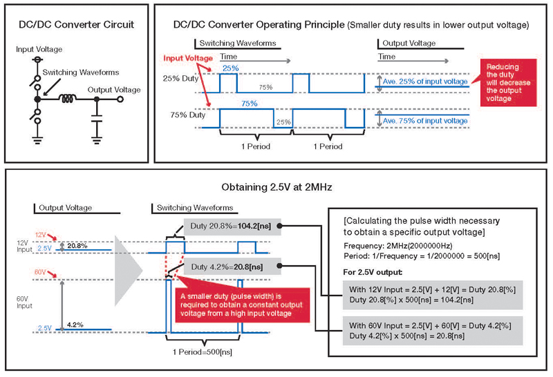
Figure 2: DC/DC converter operation
One technical hurdle for achieving lower output voltage from a higher input voltage at high frequency is narrowing the switching pulse width. The switching pulse width of a DC/DC converter is a function of the input voltage, output voltage, and switching frequency, and is calculated by the following:
t_on = V_OUT /V_IN÷f
(ton: Switching Pulse Width, VOUT: Output Voltage, VIN: Input Voltage, f: Switching Frequency)
Formula 1: Switching Pulse Width Calculation Formula
As can be seen from the above equation, the switching pulse width narrows as the input voltage increases, output voltage decreases, and frequency rises. Therefore, a method for reducing the switching pulse width is required for 48V Mild Hybrid systems. But to reduce pulse width it is first necessary to solve problems related to noise generation during switching.
When this switching noise is introduced into the IC unstable operation may occur. To prevent this, conventional control methods utilize mask time. Also, an analog circuit is required for operation, which introduces a delay time. These two factors that arise due to the increased noise component cause the pulse width to become wider.
An analog control is needed, which leverages high voltage processes and ultra-fast pulse control circuitry to detect information before noise is generated and perform appropriate control.
ROHM’s vertically integrated production system together with both proprietary analog design technology and power supply process expertise have made it possible to achieve such a narrow ON time. Nano Pulse Control devices are available capable of converting voltages as high as 76V down to 2.5V in a single stage and, therefore, achieve much higher efficiencies than when using multiple converters to meet very high step-down ratios. Another benefit of Nano Pulse Control is that the higher frequency switching circuitry (over 2MHz) results in smaller component sizes, and, consequently, a smaller circuit footprint.
MOSFET power solutions advancements for reducing RON
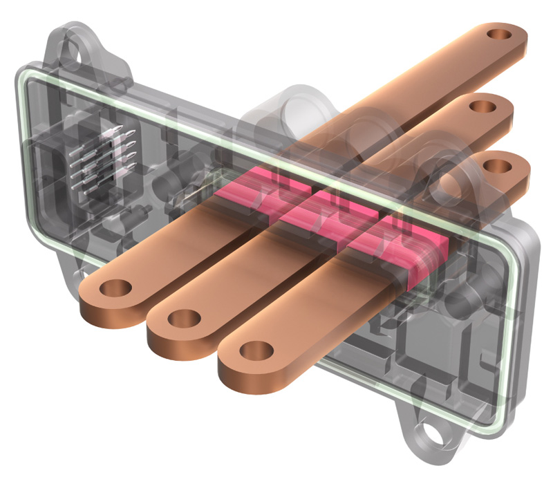
As MOSFET RON is one of the largest contributors of reducing DC/DC converter efficiency, minimizing RON is a priority in making the industry’s highest single-stage voltage conversion possible. An enabling technology for reducing RON for power MOSFETs is the use of copper clip (Cu Clip). This technology uses a solid copper bridge between the power device surface and the package leads. The benefits of Cu Clip technology range from lower RON losses to reduced inductive parasitics on the lead lines.
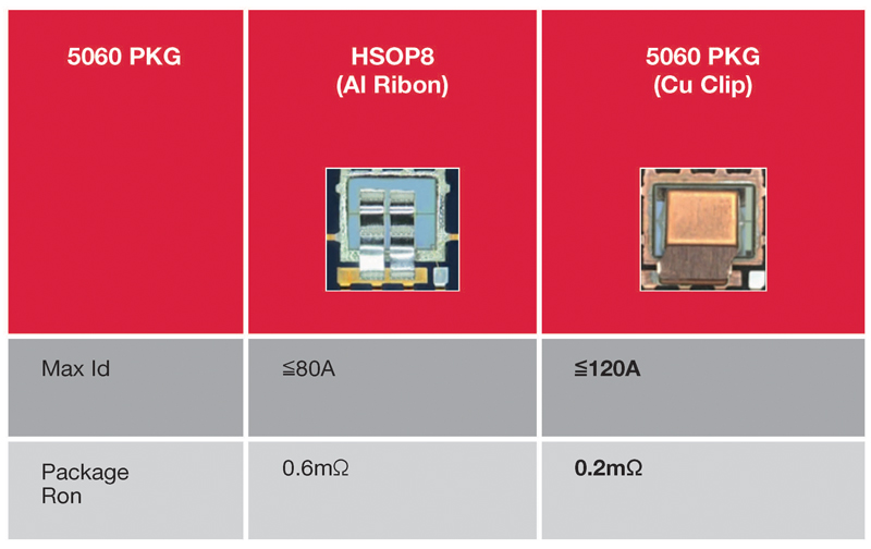
Click image to enlarge
Figure 3: A comparison of the RON and current capability of 5060 power MOSFET packages, one with conventional die bonding and one using copper clip technology
The main reason these benefits can be achieved is that the copper bridge eliminates several long and thin bond wires – along with their respective contact resistances and inductive parasitics. Moreover, Cu Clip packaging allows for more effective heat sinking of the device, that when paired with an adequate heat sink, could reduce the device’s operating temperature together with RON. As the copper forms in the Cu Clip package are large and have a high contact area with the die, they are more efficient at conducting thermal energy to a heat sink. This allows for much smaller heat sinks and an overall reduction in circuit board footprint.
Conclusion
As high voltage power rails become more prevalent and power rails for digital circuits continue to drop, there is a greater need for high efficiency DC/DC conversion. Reducing the number of conversion stages to a single stage provides a massive boost in efficiency, as does innovative MOSFET power device packaging design that reduces conduction losses. ROHM Semiconductor has been spearheading technological development in these areas and continues to release new DC/DC conversion and MOSFET devices that move away from conventional power electronics limitations and embrace the future.