Author:
Tom Ribarich, International Rectifier
Date
04/01/2014
 PDF
PDF
Typical switched-mode power converters today include circuitry for monitoring the current flowing through a switching power MOSFET or IGBT for regulating or limiting peak current levels. This is necessary to protect the switch against high peak currents that can damage components or saturate inductors. A low-ohmic resistor is typically placed in between the source of the MOSFET (or emitter of the IGBT) and ground for sensing the current. However, the power losses across this resistor can be high and system cost and size can increase significantly, especially if very high currents are being switched and heat-sinking is required. This article describes a new circuit that instead uses the RDS(on) of the MOSFET itself to directly sense current. This allows for traditional current-sensing resistors (or current-sensing transformers) and their associated power losses to be eliminated.
Traditional current sensing
The most common circuit used for sensing current flowing through a switch includes placing a low-ohmic resistor in between the bottom of the switch and ground (see Figure 1). During the switch on time, current flows through the switch, the sensing resistor, and to ground. As the current flows through the sensing resistor, a voltage drop occurs across the resistor (VCS), which is then used by another circuit for monitoring or detection purposes.
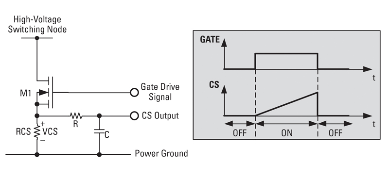
Click image to enlarge
Figure 1: Traditional resistor current sensing.
Typically there is an inductor in series with the switch that causes the current to ramp up linearly during the on-time. There is also a turn-on “spike” due to the gate-to-source current that flows through the resistor during the rising edge of the gate voltage. When the switch is off, current no longer flows and the voltage across the sensing resistor drops quickly to zero. A turn-off “spike” can also occur due to the switch capacitance currents that flow momentarily when the voltage across the switch rises again. A small low-pass R-C filter connected between the top of the sensing resistor and ground is used to suppress these on and off spikes to avoid false triggering of the detection circuitry.
Any voltage drop produced across the sensing resistor during the on time of the switch will decrease the actual gate-to-source voltage of the switch. This can increase both the on-resistance of the switch and conduction losses, and, if the currents are high enough and the voltage drop across the sensing resistor is significant, the switch can enter linear mode. Also, any inductance between the switch and the sensing resistor due to the pcb layout will cause large inductive spikes that can cause unwanted EMI and possibly damage the switch or the gate drive circuitry. Finally, depending on the value of the sensing resistor and the current levels flowing through the sensing resistor, a given power loss across the resistor will result that will reduce system efficiency and produce heat that may require thermal management.
RDS(on)current sensing circuit
The new RDS(on) sensing circuit eliminates the traditional series-connected sensing resistor and is connected instead in parallel to the power switch. The circuit measures the RDS(on) of the switching power MOSFET, or VCE(on) of an IGBT. The sensing circuit has four external connection nodes (VS, GATE, CS, COM) and includes (see Figure 2): a 600V MOSFET (HVFET); an RC-delay circuit (R1, C1, D1); and a PMOS hold-down transistor (Q1). The circuit does not require a VCC supply node and instead utilizes the existing gate drive signal for powering and turning the circuit on and off. During the off time of M1, the gate drive signal is at COM, the HVFET is off, Q1 is on, and the CS node is held at COM.
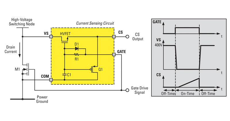
Click image to enlarge
Figure 2: New RDS(on) or VCE(on) current sensing circuit.
Since HVFET is off, any high voltage occurring at the drain of the power MOSFET will be safely blocked by HVFET from the rest of the low-voltage circuitry. When M1 is turned on by the gate drive signal, the drain voltage of M1 will decrease to a level given by the current flowing through M1 multiplied by the RDS(on) of M1. After a short delay time set by the RC-delay block, the gate voltage of the HVFET rises up and turns the HVFET on. Q1 turns off, therefore releasing the CS output node. The drain voltage of M1 is then transmitted across HVFET to the CS output node. The voltage at the CS node then becomes the desired current-sensing signal from the RDS(on) or VCE(on) of M1.
When the gate drive signal of M1 goes low again, M1 turns off. The gate of HVFET gets discharged quickly through D1 and HVFET turns off to once again block any high voltage occurring at the drain of M1. The CS output node is then held at COM again through Q1. Assuming the drain of M1 is a typical high-voltage switching node that is connected to an inductor, the voltage signal produced at the CS output node will be the same sawtooth waveform that would result from using a traditional current sensing resistor placed at the source of M1. The CS output node can then be fed to a comparator circuit or other desired current-sensing functions of a PWM controller or MCU circuit.
The measured waveforms (see Figure 3) show the functionality of the new circuit and the desired current sense signal at the CS node at room temperature. Compared to the conventional resistor sensing method, both methods match the actual current shape and both exhibit noise spikes due to switching. Proper filtering or digital blanking of the final PWM or MCU current sensing circuit will easily ignore these noise spikes to prevent any false triggering. Also, it is well known that the RDS(on) of the power MOSFET will increase with increasing ambient temperature and therefore cause an error in the CS measurement. Therefore, on-going application work is currently being done to compensate for temperature with additional circuitry.
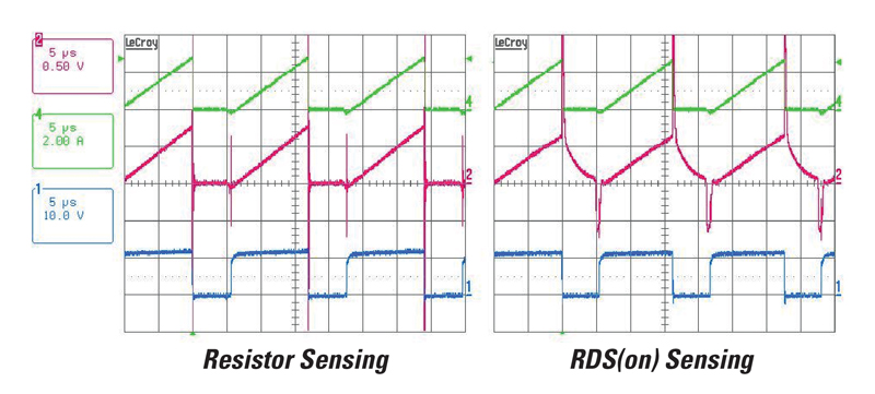
Click image to enlarge
Figure 3: Resistor vs. RDS(on) current sensing waveforms.
Switch drain current (upper trace), CS measurement (middle trace), gate drive signal (lower trace). Resistor = 0.27ohms, MOSFET RDS(on) = 0.25ohms.
Since no VCC node is required for this circuit, the pcb layout becomes very simple to design (see Figure 4). The new current sensing circuit has been realized in a tiny SOT-23 IC, the IR25750L. The IR25750L can be placed conveniently next to the power MOSFET or IGBT and connected easily to the existing pcb traces that are already used for the power switch (GATE, DRAIN, COM). Only the CS trace needs to be routed back to the main PWM controller or MCU of the power supply.
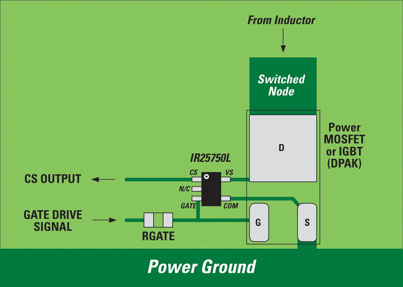
Click image to enlarge
Figure 4: IR25750L typical surface-mount pcb layout.
Conclusion
The IR25750L current sensing IC offers a novel method for sensing current and eliminating traditional series-configured current sensing resistors or current transformers. This parallel-connected configuration and small SOT-23 package enables ease of pcb layout and routing, especially if several switches are being monitored. The uses for this new current-sensing device spans across all applications of switched-mode power electronics and the benefits of eliminating cost, shrinking board space, reducing power losses, and increasing overall efficiency are enormous.