Date
06/04/2015
 PDF
PDF
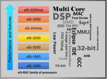
the eSI-32X0MP scalable, asymmetric multicore processor
EnSilica, a leading independent provider of semiconductor IP and services, has added to its family of eSi-RISC processor cores with the launch of the eSI-32X0MP scalable, asymmetric multicore processor. The eSi-32X0MP targets applications requiring a high level of processing per MHz and low power consumption in a small footprint, such as low-power WiFi, LTE Cat-0 and other IoT standards as well as scalable sensor (touch screens and intelligent sensors), Gbit security protocol and solid state disk levelling algorithm processing.
A typical configuration of the eSi-32X0MP to address wireless/cellular standards comprises an asymmetric dual core processor. One processor is optimized for implementing physical layer (PHY) processing and the second core is optimized for running an advanced protocol stack. However, the eSi-32X0MP can be configured with an unlimited number of processors depending on the application. Indeed, an early implementation already in production is a seven core eSi-3250MP for multi-gigabit packet processor acceleration.
The eSi-32X0MP’s PHY core provides advanced DSP acceleration with dual-MAC and SIMD instructions for complex arithmetic as well as fast divide, square root and log calculation acceleration. The second core’s advanced protocol stack accelerates various bit field operations, such as fast insertion and extraction, and a cyclic redundancy checker (CRC).
The processor sub-systems can be enhanced for symbol level processing including FFT/IFFT, DFT, Viterbi and Turbo decoding using optional hardware accelerators from EnSilica's eSi-Comms IP library. Security layers can be implemented with the aid of a memory protection unit (MPU), True random number generator (TRNG) and optional hardware accelerators for Snow3G, AES, RSA and ECC from EnSilica’s eSi-Crypto IP library.
For advanced power saving, the eSi-32X0MP implements both clock and power gating. Power gating is supported through a UPF-based (Universal Power Format) design compatible with standard front and back-end EDA tool flows. Load-locked and store-conditional instructions are provided to support inter-core communications. Both the processor and tool chain fully support multicore debug.
Each core can deliver up to 3.72 CoreMark per MHz and, when speed optimized in TSMC’s 28nm HPC process, can be clocked at over 1GHz with a dynamic power of only 14.4µW/MHz per core. When optimized for power the dynamic power for each core is only 5.09µW/MHz.
“The eSi-32X0MP is ideal for implementing low-power WiFi and wireless/cellular IoT standards such as LTE Cat-0,” said Ian Lankshear, CEO of EnSilica “The multicore architecture delivers exceptional processing performance at mature geometries. For example, an 180nm dual core configuration can deliver 500 MIPS for a gate count of less than 50k NAND equivalent gates.”
"Adopting the highly compact eSi-32X0MP asymmetric dual processor architecture for our touch screen controllers has facilitated the development of a novel high-performance IC solution for high-end applications without having to move to a more advanced process geometry,” said Ken Tsui, Vice President, Design Engineering of Solomon Systech Limited.
"The eSi-32X0MP provides us with an optimized platform to address IoT wireless standards with two highly coupled cores, each accelerated for the task in hand but still benefiting from a shared development tool chain,” said Dr Sondur Lakshmipathi CEO of Mymo Wireless. “Additionally, EnSilica’s eSi-Comms IP suite is fully integrated providing acceleration for symbol level processing operations."