Ensuring EMC in High-Density Automotive Lighting

Advanced LED and OLED lighting systems are now essential to the safety and functionality of next-generation vehicles.
Figure 1: Block diagram of the L99LDLH32 smart lighting driver
OLEDs provide thin profiles and uniform light diffusion, while LEDs are known for their brightness and efficiency, reshaping the visual dynamics of modern vehicles. However, with modern E/E architectures becoming increasingly complex, systems are significantly more susceptible to electromagnetic interference (EMI) which is a fundamental concern in electromagnetic compatibility (EMC).
EMI is a complex phenomenon where unwanted electrical noise disrupts and may compromise the normal functioning of electronic devices, which can potentially threaten the sophisticated electronic systems essential to modern vehicles. For example, in automotive exterior lighting applications, long cables connecting the battery to digital LED modules or OLED panels can act as unintentional antennas, capturing EMI from the surrounding environment.
This interference can cause fluctuations in control signals resulting in visible light flickering, erratic dimming functions, and corruption of the intricate communication protocols managing the lighting data. Continuous exposure to EMI is very dangerous because it can even stress electronic components, reducing their lifespan and leading to premature failure.
Integrated Driver Design for EMI Mitigation
Engineered specifically to mitigate EMI, the L99LDLH32 is an intelligent high-side driver designed to power next-generation automotive OLED and LED lighting applications. Encapsulated in a compact 7 mm x 7 mm QFN package, it integrates 32 regulated current sources.
Each source can be programmed to deliver a specific current, enabling independent and precise control of individual pixels. Furthermore, the device adheres to Automotive Safety Integrity Level (ASIL) B requirements as per ISO 26262 regulations, ensuring a high standard of safety.
The driver employs high-frequency PWM technique combined with programmed 8-bit resolution current for exact light-intensity control. To minimize noise, designers can synchronize the PWM for all channels using a single bit. This strategy effectively reduces the sudden electromagnetic energy surge that occurs when multiple channels switch simultaneously, lowering the likelihood of EMI with other electronic in-vehicle systems.
Additionally, a built-in CAN FD Light protocol handler and transceiver streamlines connectivity, eliminating external components like timing crystals. This protocol supports data rates up to 1 Mb/s, allowing smooth dimming transitions crucial for reducing electrical noise.
Advanced Clock-Dithering Techniques
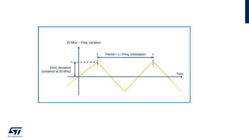
Rapid switching of LEDs is a primary EMI source. To mitigate this, the L99LDLH32 integrates a programmable clock-dithering function that modulates the frequency of the internal 20-MHz oscillator. By applying a triangular waveform to the oscillator, the frequency is smoothly shifted up and down.
Click image to enlarge
Figure 2: Oscillator dithering curve
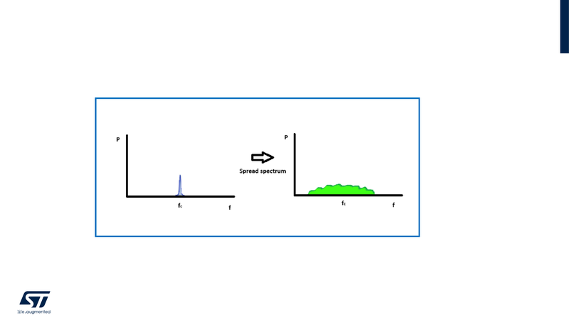
This waveform ensures linear and predictable frequency changes, which induces a dithering effect that spreads the noise across a wider range of frequencies. Consequently, this diminishes the peak amplitude of noise at any individual frequency by dispersing the energy from the fundamental frequency and its harmonics over a broader spectrum.
Click image to enlarge
Figure 3: Spread spectrum effect
Users can configure the frequency modulation and deviation using three dedicated bits, selecting from eight distinct configurations. For instance, a dithering setting of 100 corresponds to a frequency modulation of 19.5 kHz and a frequency deviation of 6.5%.
Device-Level Conducted Emissions: The 150 Ω Method
EMC testing guarantees devices perform efficiently without generating or succumbing to EMI. The BISS (Bosch / Infineon / Siemens Specification) standard categorizes testing into conducted and radiated RF tests and specifies certain limits about global and local pins and also defines these ones. Section 4 of IEC 61967 specifies the 150 Ω testing method for evaluating conducted electromagnetic emissions directly at the device's pins.
Based on IEC 61000-4-6, a cabling network represents in most cases antennas with 150 Ω impedance. A termination network of 150 Ω ± 20 Ω is used for accurate results.
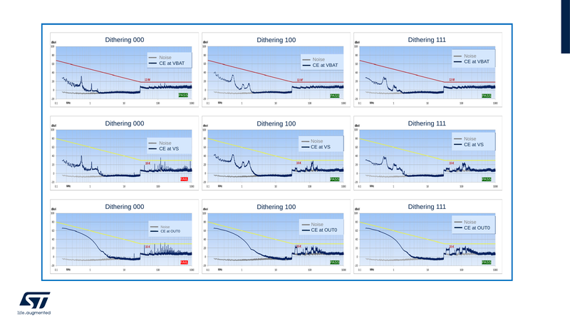
Conducted emissions (CE) measurements were conducted on global pins, which carry signals or power, which enters or leaves the application board without any active component in between, such as the battery supply (VBAT). Local pins, instead, which carry a signal or power, do not leave the application board and they were also tested, including the input supply voltage (Vs), external pre-regulator pin (VPRE_REG), temperature sensor voltage (NTC), and output pin (OUT0). Experimental evaluations of the L99LDLH32 were performed under various dithering conditions.
Click image to enlarge
Figure 4: Conducted emissions measurements at different coupling points
The data clearly indicated that setting 000, where no dithering is applied, is significantly less effective in managing conducted emissions. In contrast, settings 100 and 111 successfully dispersed the noise, proving to be the preferable choices for applications demanding stringent EMI control.
Ultimately, the driver successfully met also all peak limits imposed by CISPR 25 class 5 for broadcast bands (such as Long Waves, Medium Waves, and FM) and mobile services (like Citizens Band and VHF).
Device-Level Immunity: Direct Power Injection (DPI)
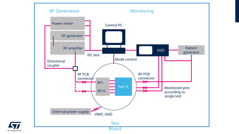
To assess susceptibility, the Direct Power Injection (DPI) test (IEC 62132-4) determines the lowest level of power disturbance required to affect the standard functioning of an IC. An RF disturbance signal, spanning a frequency spectrum from 150 kHz to 1 GHz, is introduced directly into an IC pin via a coupling capacitor.
Click image to enlarge
Figure 5: Schematic of the typical test setup for DPI measurements
For the L99LDLH32, disturbances were coupled using passive components (120 Ω and 51 Ω resistors, and a 6.8 nF capacitor) with a maximum tolerance of 1%. The failure criteria during the DPI test monitored critical internal functions: the 5 V LDO output (communication interface regulator) and the 3.3 V LDO output (logic and I/O regulator) were limited to a ±3% variation, while the output current (I_OUT0) was limited to a ±11% variation for 250 μs.
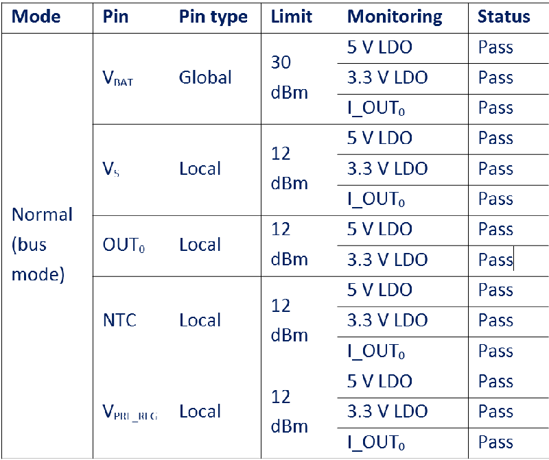
Click image to enlarge
Table 1: DPI measurement results
The experimental results confirmed the device's robust immunity: global pins successfully withstood tests up to 34.7 dBm (against a 30 dBm limit), while local pins maintained stability up to 30 dBm (well beyond the 12 dBm requirement). This performance guarantees the reliable operation of critical communication and logic components even under severe RF stress, making the driver an ideal choice for electromagnetically noisy automotive environments.
System-Oriented Resilience: Bulk Current Injection (BCI)
While device-level tests isolate the IC, the Bulk Current Injection (BCI) method performs system-oriented measurements to evaluate noise immunity within the vehicle's actual electrical environment. Adhering to standards like IEC 62132-3 and Volkswagen's VW TL-81000/2018, BCI injects disturbance signals into the wiring harness using a current injection probe that acts as a current transformer.
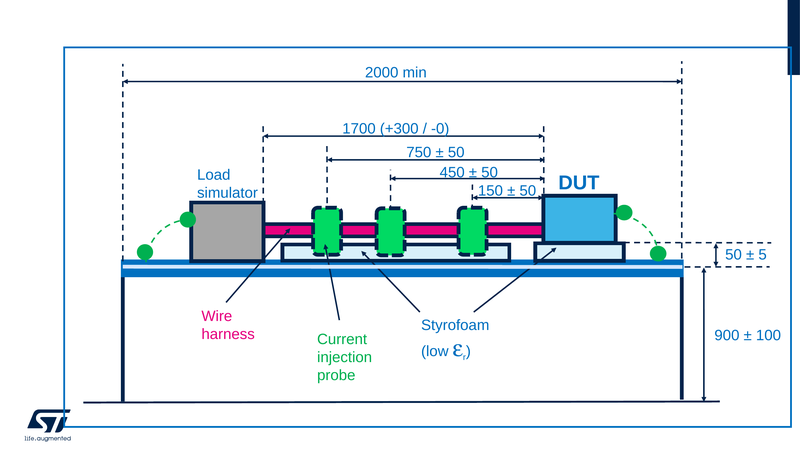
Click image to enlarge
Figure 6: Diagram of the BCI substitution method test configuration
The testing utilized an evaluation board featuring two L99LDLH32 devices operating a 32x32-pixel OLED panel.
The BCI disturbance current was introduced into four wires corresponding to the high and low input/output voltages of the CAN bus (CAN_H and CAN_L), the battery supply voltage (VBAT), and the ground connection.
Before the test starts, injecting probe must be calibrated, so the net incident power was measured to generate a specific current profile. Then the injection power follows the profile obtained during calibration which requires up to 106 dBμA for frequency ranges like 15 to 54 MHz for instance. The criteria for identifying faults were strictly visual and functional. In Bus Mode, a minimum of 31 out of 32 pixels in a row had to remain lit with no visible change in brightness when RF power was applied. When transitioning to Fail-Safe Mode, exactly 29 pixels were expected to switch off, leaving only two illuminated. During testing, the L99LDLH32 exhibited no light-intensity fluctuations and maintained stability without erroneously shifting into fail-safe mode, even when subjected to RF power levels up to 7.5 W across the full 1 to 400 MHz frequency range analyzed.
.jpeg)
 Single.jpeg)