Author:
Susheel Badha, Applications Engineer and Mahmoud Ismail, Senior Application Marketing Expert both at Infineon Technologies
Date
06/08/2021
 PDF
PDF
Click image to enlarge
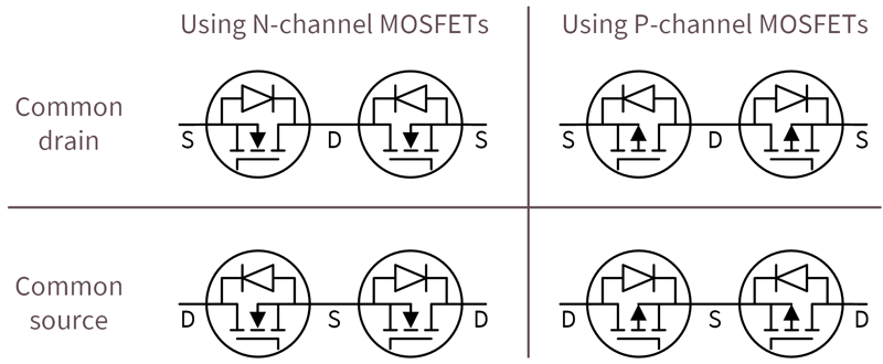
Figure 1. BDPS configurations
The global market for battery-powered applications is rapidly growing, including power tools, consumer robotics, light electric vehicles, and many others.
The evolution of switched-mode power supply (SMPS) topologies enables designers to ensure safe charging and discharging of the equipment’s battery using bidirectional converters through the same terminal. However, to meet the safety requirements and prevent damage and failures, those SMPS need to be equipped with a protection switch. Uni- and bidirectional switches are widely used to charge/discharge and protect against various failures like in-rush current, overcurrent, short-circuit, reverse voltage, or over-and under-voltage.
In the following sections, we present the guidelines that can help designers to develop an appropriate unidirectional, or bidirectional direction protection switch circuit such that the MOSFETs are operating within their safe operating area.
A bidirectional switch is an active switch that has the ability to block the current in both directions. It offers effective protection against abnormal conditions like a short-circuit, reverse voltages, etc., that occur accidentally or due to manual errors in battery/SMPS terminals.
A BDPS can be realized by using two N- or P-channel FETs. N-channel FETs are preferred out of these two due to low RDS(on) and cost compared to P-channel FETs. Because of the body diode, a single MOSFET can pass or block the current in only one direction. The configurations shown below in Figure 1 are required to realize a BDPS.
To enhance efficiency, battery backup duration, effective protection against failures, and to avoid the cost of thermal solutions, MOSFET selected for BDPS shall offer:
Considering the various parasitic effects, the MOSFETs used for BDPS ensure their safe operation in normal and abnormal cases that a certain application can expect. Below is the high-level schematic of a system with a battery, a load, and a BDPS. Additionally, various wires and parasitics are modeled. A worst-case scenario depicted in a short circuit event is analyzed to correctly select the type and amount of MOSFETs for the BDPS.

Click image to enlarge
Figure 2. MOSFETs topology as low-side BDPS
Click image to enlarge
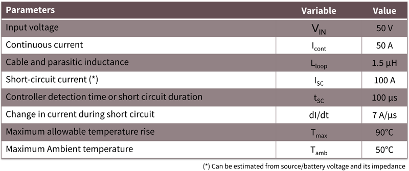
Table 1. Detailed design parameters assumed in this article to illustrate the MOSFET selection for BDPS
Typically MOSFETs used as protection switches are programmed to turn on slowly to limit inrush current and turn off as fast as possible to protect against abnormal conditions (such as a short-circuit or an overcharge etc.). During turn on/off, MOSFETs shall be operated within the safe limits as per chapter “ Safe operation of MOSFETs.”
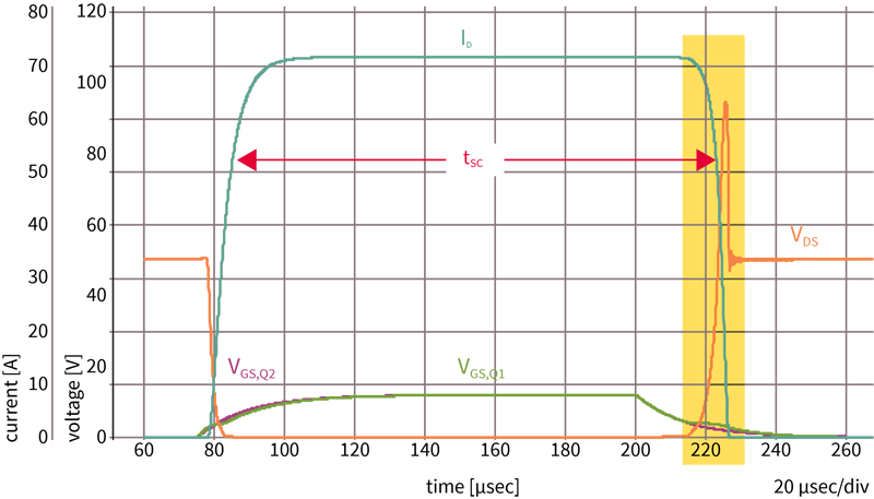
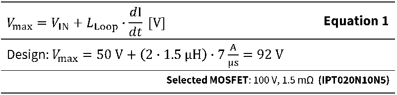
The fast switching off of MOSFETs in the events like a short-circuit leads to high dI/dt currents through the loop inductance and induces high voltage (VL = L*dI/dt). Eventually, this voltage adds to the drain voltage of the MOSFET (as shown in Figure 3), which could lead the MOSFET into avalanche. The maximum voltage across the MOSFET used in the protection switch can be calculated by Equation 1. To avoid MOSFET avalanching, the breakdown voltage of the selected MOSFET needs to be higher than the maximum voltage (Vmax) calculated. In this case, IPT020N10N5, an OptiMOS™ 5 100V power MOSFET in TO-Leadless (TOLL) package, is selected.
Click image to enlarge
Figure 3. Typical waveform during short-circuit
Click image to enlarge
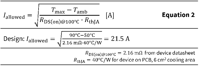
Equation 2 calculates the maximum current (IAllowed) that a MOSFET can carry at the maximum operating temperature allowed by each application.
Click image to enlarge
From Equation 2, it can be noted that a MOSFET with lower thermal resistance allows for higher current through it.
Infineon’s MOSFET portfolio is available in different packages offering various thermal resistances. (Figure 4).

Click image to enlarge
Figure 4. MOSFET package area vs. thermal resistance vs. current
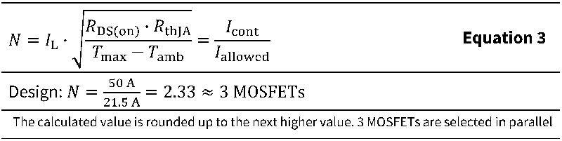
Typically, MOSFETs are paralleled for high-current applications to reduce losses and distribute temperature evenly on the PCB.
Equation (3) estimates the number of MOSFETs in parallel (N) that can achieve the desired operating temperature.
Click image to enlarge
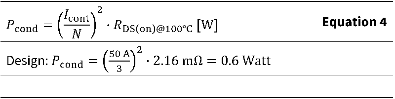
MOSFETs have a positive temperature coefficient, meaning that RDS(on) increases with the device temperature.
Due to I2R or conduction losses, the die temperature of the MOSFETs increases. But the temperature of the MOSFET with low RDS(on) shares a higher current, and its RDS(on) increases due to higher I2R losses, resulting in a stable thermal state after a specific duration.
However, the MOSFET with the lowest RDS(on) is the hottest one, and it must be ensured that the temperature on this MOSFET shall be less than the operating temperature specified in its datasheet.
Conduction or I2R losses (Pcond) of a MOSFET is the lone contributor to the losses in a BDPS. MOSFETs best-suited for BDPS offer best-in-class low on-resistance (RDS(on)). As discussed previously, the RDS(on) of the MOSFET increases with increasing temperature. For safe operation, MOSFETs are mainly operated below 100°C. Considering the RDS(on) of MOSFETs at 100°C, the conduction losses of the MOSFET can be calculated using Equation 4.
Click image to enlarge
Due to its more than 40 years of MOSFET experience and continuous package and technology innovation, Infineon can offer decreased RDS(on) values when moving from OptiMOS™ 3 to OptiMOS™ 5 in the same package to enable better performance in applications such as BDPS where low RDS(on) is critical.

Click image to enlarge
Figure 5. RDS(on) improvement over Infineon MOSFET technologies and generations
The maximum allowable temperature rise on the device depends on the application area. Case temperature of the MOSFET is calculated from Equation 5.
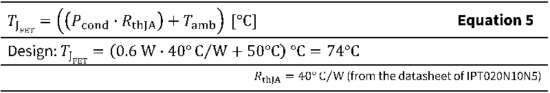
Click image to enlarge
The estimated temperature on the MOSFET is below the maximum allowable temperature rise (Tmax) on the devices (i.e., 95°C) and satisfies the design requirement.
Usually, housekeeping ICs (such as battery monitoring ICs, comparator ICs, etc.) or controllers are employed to detect faults and control protection switches. These controllers need time to detect and respond to the faults. In the case of a short-circuit (as shown in Figure 3), MOSFETs shall withstand and shall not fail for such response periods (Tsc).
A slow turn-on of protection switches is mainly preferred to limit in-rush current and the fast turn-off to protect against faults. During this turn-on/off time, MOSFETs are subjected to pass through linear mode operation (highlighted by the yellow shaded region in Figure 3). The MOSFETs selected as protection switches must be carefully analyzed for:
Short high-current pulses during a short-circuit period (Tsc) or short high-power dissipation during inrush current limiting period can create a hot spot on the MOSFET die. To ensure safe operation, the transient junction temperature of the MOSFET must below the silicon operating temperature specified in the device datasheet.
Equation 6 below uses the transient thermal impedance from the datasheet to estimate the junction temperature on the FET.
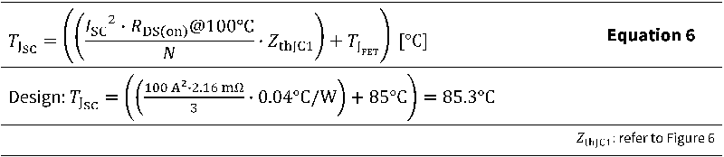
Click image to enlarge
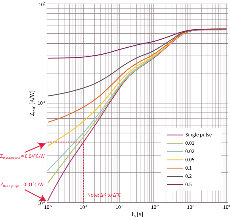
Click image to enlarge
Figure 6. IPT020N10N5 ZthJC at 100 μs
During a turn-on/-off event, the MOSFET used as the protection switch accommodates linear mode operation. Under abnormal conditions such as, for example, a short-circuit, a safe design ensures a MOSFET operation within its safe operating area (SOA).
In MOSFETs datasheets, SOA boundaries are defined at a specific squared pulse duration. As explained in [1], the protection switch operates at certain dV/dt or dI/dt, which means that non-squared power pulses are applied during turn-on/off.
So, it is not possible to use the SOA chart from MOSFETs datasheets directly. Instead, in case of critical and abnormal conditions, one should perform the following calculation steps:
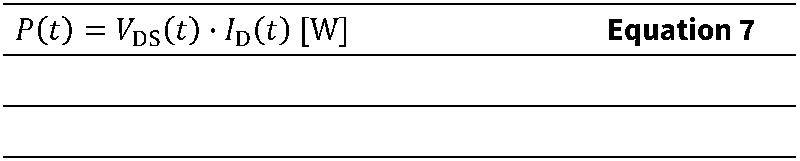
Click image to enlarge

Click image to enlarge
Figure 7. VDS(t), ID(t), and PD(t) waveforms
Click image to enlarge

Click image to enlarge
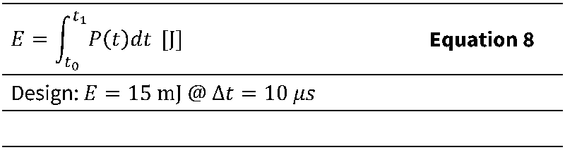
Figure 8. Energy dissipation
Click image to enlarge
Click image to enlarge
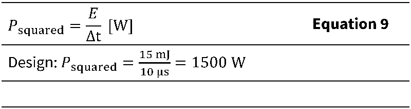
Figure 9. Squared power dissipation
Click image to enlarge
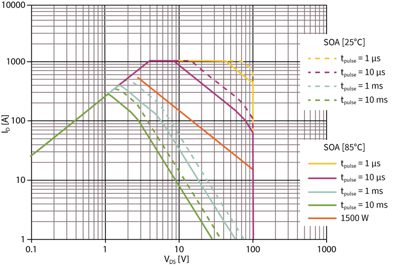
Figure 10. Derated SOA chart of IPT020N10N5
Based on the above, one can conclude that the design is safe because the estimated squared power line (1500 W at 10 μs) is far below the SOA limit at tpulse = 10 μs.
Click image to enlarge
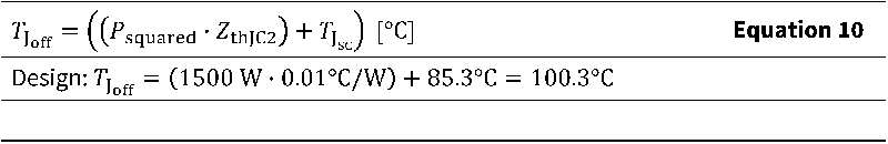
In this case, during switch-off, MOSFET’s temperature rises to 100.3°C, which is below the operating temperature of 150°C.
When it comes to ensuring a safe and reliable MOSFET performance in a protection switch application, various factors come into account. Key considerations for proper MOSFET selection for this very application area must include low power dissipation, excellent thermal interface, avalanche-free operation, identical current sharing between parallel MOSFETs, and proper and safe turn-on/off operation.
In this article, Infineon presented a framework for designing a protection switch for unidirectional or bidirectional direction protection switch circuits such that the MOSFETs are operating within their safe operating area.
To explore Infineon’s MOSFET offering and broad solution portfolio for protection switch applications, please visit our Battery Management System related web page and our Power MOSFET related web page.
[1] Application Note v1.1, Infineon Technologies AG, “Linear Mode Operation and Safe Operating Diagram of Power-MOSFETs,” May 2017