ESD Protection: How to Design Safer Consumer Electronics
Consumers are the single biggest risk to electronic devices
Consumers are the single biggest risk to electronic devices such as Smartphones and Tablets that play a vital role in their lives. Not only because they might drop them on the floor, but also because human touch to any device containing sensitive electronic semiconductors can be the source of an ESD (Electro Static Discharge) event. Hence, only utilizing proper circuit protection in the design process can ensure the longevity of electronic devices, whether used at home, at work, or in the car.
ESD events can be traced to a phenomenon known as triboelectric charging. Triboelectric charging occurs when two materials make contact and then are quickly separated. Electrons are transferred between the two materials resulting in one being positively charged and the other negatively charged. This resulting ESD build-up depends on several factors such as area of contact, the speed of separation, relative humidity, chemistry of the materials, etc. This process occurs thousands of times per day and mostly goes unnoticed unless the discharge is sufficiently severe enough to cause some mild, brief discomfort (e.g. walking across carpet and grabbing the door handle). The charges generated can range from hundreds of volts to tens of thousands of volts.
ESD exposure is a real problem in today’s sophisticated consumer equipment, due to ever shrinking board level chipset size and thus the resulting silicon geometry via wafer processing. ESD structures have become too large and costly to be included in the silicon IC package; therefore, the IC suppliers have removed or greatly reduced the internal ESD protection. However, once these ICs are installed in consumer products, they may be subjected to ESD events that are not as well controlled as they are in manufacturing environments.
Traditional ESD test models: not harsh enough?
IC manufacturers have historically used an ESD test model (MIL-STD-883, Method 3015: Human Body Model) that relates specifically to a manufacturing environment while equipment manufacturers concerned with ESD events in the field have used a harsher model as defined by the IEC (International Electrotechnical Commission), namely the IEC 61000-4-2 standard. As of this writing, the majority of IC suppliers test their products at 500V with the Human Body Model (HBM) while end equipment manufacturers will test at 8000V (and beyond) using the IEC61000-4-2 standard.
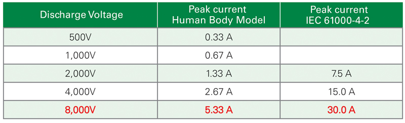
Figure 1 shows a comparison between HBM (Human Body Model) ESD currents that many chipset providers will use versus the environmental ESD events outlined in IEC 61000-4-2 that many consumers will unknowingly inject into their consumer devices:
Click image to enlarge
Figure 1 ESD Events Outlined
One can see that the worst case HBM ESD level is much lower than the worst case ESD current level for the IEC61000-4-2 (highlighted in red). The 8kV event described in IEC 61000-4-2 compared to the same 8kV event described in the HBM has a 5.6x increase in current. A chipset that survives HBM testing (manufacturing environment test conditions) is not guaranteed to survive in the field, where the ESD exposure will be much more severe. Finally, as mentioned previously, most IC suppliers only test to 500V via the Human Body Model and compared to an 8kV ESD transient in the field, the chipset will see a near 100 fold increase in current certainly sealing its fate unless ESD protection is added to the design.
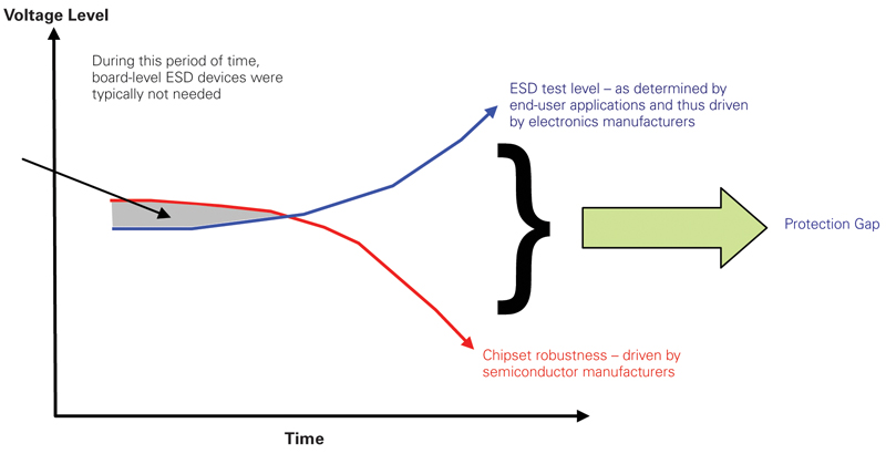
Over the last several years, application-testing requirements have become more and more severe with an ESD event of 8kV being the lowest level typically used now. Testing levels are trending towards 20kV and even 30kV while IC suppliers have continued to remove protection to save silicon area for more functionality. Figure 2 shows the “gap” between chipset ESD capability vs. the ESD exposure level in field applications and points to the growing need for supplementary ESD protection.
Click image to enlarge
Figure 2: ESD testing
Proper ESD protection is crucial
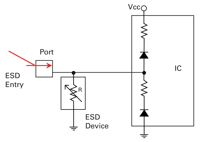
Selecting the correct ESD protection device (typically referred to as a TVS Diode Array) is vital for ensuring the end application will survive and continue to function as originally designed. The dynamic resistance is a very important ESD protector parameter, if not the most important, to consider when selecting a protection component. Any protection solution has an intrinsic resistance value associated with its clamping characteristic. An ideal solution minimizes the intrinsic resistance so that a protection solution has the lowest impedance path to ground during a surge event.
Figure 3 describes this issue. During an ESD event the clamping device will turn on, or go from its nominal state of high impedance to one of low impedance. If its series resistance is high, a high voltage (V = I*R) develops across the component, thus providing less effective protection of the IC its protection. If this series resistance is low, the voltage developed across the protection component is lowered and thus the exposure level to the IC is lowered.
Click image to enlarge
Figure 3: Protected IC
This lower dynamic resistance (resistance value of the protection component during clamping mode) allows more of the surge current to be routed away from the IC and into ground as depicted in this diagram below. Littelfuse TVS Diode Arrays are designed to attain the lowest dynamic resistance value thus minimizing the overall voltage drop across the protection component and maximizing the current through it instead of through the protected IC.
In general, silicon protection devices will provide the best ESD protection due to their inherently lower dynamic resistance compared to competing technologies such as polymers, ceramics, etc. The typical dynamic resistance of silicon components will range from 0.2-3.0Ω depending on the supplier while ceramic type solutions (of equal capacitance) offer dynamic resistances in the range of 2Ω to 5Ω on average.
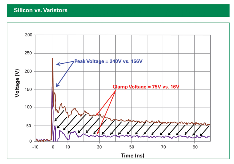
The graph in Figure 4 shows the “let-through” energy difference between a silicon component and its varistor counterpart when an 8kV ESD transient is injected into each component. One can see the leading edge turn-on difference and the final clamping voltage differences in this chart below. The difference between the curves (the arrows) is the resulting energy the IC or chipset must successfully survive to prevent potential damage or premature failure.
Click image to enlarge
Figure 4: Silicon vs. Varistors
International standards
Consumer electronics such as LCD TVs, smartphones, tablets, eReaders, set top boxes, gaming consoles, digital cameras, audio players, etc are seemingly unlimited and constantly evolving. Nonetheless, the ports, or interconnects, on these devices are quite common and require ESD protection since they are the interface to the outside world.
Some device functions will require compliance to country safety standards thus needing overcurrent and overvoltage protection. Other functions may need protection from environmental factors such as ESD, but also nearby lightning surges, or EFT (electrically fast transients) caused by nearby high inductive load equipment cycling on and off (e.g. a vacuum cleaner).
Products that are directly connected to the AC mains (120 to 250VACrms) may be exposed to severe surge transients (lightning, load switching, etc.) and short circuit/overload conditions. This requires a combination of overcurrent (fuses or PTCs) and overvoltage (MOVs, TVSs, or TVS diode arrays) components due to the severe exposure.
Standards that may specifically require this protection are:
1) IE 61000-4-4 (EFT user level environment)
2) IEC 61000-4-5 (lightning induced surges)
3) IEC/EN 60950-1 (safety standard)
Portable consumer products that contain an ac or dc adapter may have specific ESD and low-level lightning exposure threats that must be accounted for.
Standards that may specifically require this protection include:
1) IEC 61000-4-2 (ESD user level environment)
2) IEC 61000-4-5 (lightning induced surges)
Keypads or other manual type interface buttons may be an entry point for the destructive energy of ESD. Audio lines may have similar type ESD exposure due to the speaker wire connections and exposure to manual handling. The connectors for S-video, Composite video, HDMI, are also susceptible to ESD exposure due to the manual handling of such equipment parts. Battery pack applications will endure similar ESD exposure as well as potential “overcurrent run-away” conditions that must be protected against (IEC 61960 & IEC 62133 specifically apply). Low speed and high speed data lines have an ESD exposure and depending on their actual placement may also be exposed to lightning induced surge events.
National Standards that would typically apply for these types of applications include:
1) IEC 61000-4-2 (ESD user level environment)
2) IEC 61000-4-5 (lightning induced surges)
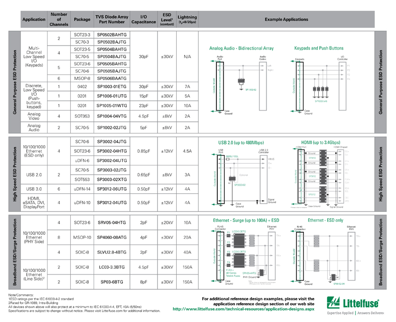
Figure 5 shows potential solutions for each of the various consumer product function types. As IC designers try to pack more functionality into smaller chipsets, ESD survivability has decreased significantly. Today, consumer products face high risks of being damaged due to overvoltage transients such as ESD, which makes it necessary to use external protection components.
Click image to enlarge
Figure 5: ESD and Port Protection Design Guide
TVS Diode Arrays not only meet the small footprint requirements, but also provide very low clamping voltages, compared to competing technologies, capable of safe guarding state of the art ICs. Exposure to EFTs, nearby lightning strikes and potential power fault events also require specific attention to overcurrent and overvoltage protection solutions. By employing the correct overcurrent (fuse or PTC) and overvoltage protection components, manufacturers can ensure their products remain an integral part of their consumer’s life.
When it comes to testing, international standards set high bars for safety and are therefore more reliable than traditional test models. The correct choice of protection components also insures the applications comply with the appropriate regulations for both safety and functional reasons.