Exploring the trends in Gallium Nitride device development
In the last few years GaN based devices, both discrete FET’s and MMIC’s, have been released and widely used in high power microwave amplifier systems. These devices, available from several foundry sources, are typically fabricated on 100mm SiC wafers. GaN on Si processes are also under consideration, however the relatively poor thermal and electrical conductivity of Si offsets the cost advantages in high performance, high reliability applications. These devices feature gate lengths as small as 0.2 microns and thus support operation into the millimeter-wave frequency bands. GaN based devices have now largely replaced Gallium Arsenide (GaAs) and Lateral Diffusion Metal Oxide Semiconductor (LDMOS) devices in all but the most cost sensitive, lower frequency applications.
GaN devices are of interest to the RF power amplifier designer because they support very high operating voltages (3 to 5x those of GaAs), and roughly double the allowable current per unit of FET width as compared with GaAs. These characteristics have an important consequence to the power amplifier designer, specifically a higher load impedance for a given output power level. Previous GaAs or LDMOS based designs often had extremely low output impedances relative to typical system impedances of 50 – 75 ohms. Low device impedances place limits on achievable bandwidth, i.e. as the required impedance transformation ratio between the amplifying device and its load increases, the number of components and insertion loss increase as well. Due to these high impedances, early users of these devices were in some cases able to achieve partial results by merely installing one in an unmatched test fixture, applying DC bias and an RF drive signal.
GaN devices are also finding their way into high reliability space applications due to these operating characteristics and their exceptional reliability. Life test data from several sources of these devices predict mean time to failure times (for single devices) in excess of one million hours at junction temperatures of 225 degrees C or higher. This exceptional reliability is mainly due to the band gap value for GaN (3.4 for GaN vs. 1.4 for GaAs). This makes them more than suitable for high reliability applications.
The chief impediment to wider use of GaN in high power applications has been its relatively high fabrication cost, typically 2 to 3 times that of GaAs and 5 to 7 times that of LDMOS based devices. This has usually been a deal breaker in very cost sensitive applications such as wireless infrastructure and consumer handsets. GaN on Si substrate processes are available, albeit with the performance issues mentioned above, and are probably best suited for these cost sensitive applications. In the near future, cost reductions, perhaps on the order of 50%, are expected due to the move to larger wafer sizes, 150mm and above, now underway at several leading sources of GaN devices.
Solid-state amplifiers for Traveling Wave Tube (TWT) replacement
Currently deployed radar systems for weather prediction, target acquisition / identification use TWT based radio frequency power amplifiers operating at C and X band. These amplifiers feature very high operating voltages (10 – 100kV), and temperatures and are susceptible to damage from excessive vibration and shock. Actual fielded reliability is thus typically 1200 to 1500 hours and leads to high maintenance, sparing, and depot costs.
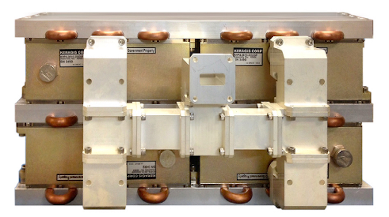
To address this application, ADI has developed an X Band, 8kW solid-state power amplifier based on GaN technology. The design uses an innovative, layered combiner approach to sum the RF power of 256 MMICs, each developing approximately 10 watts. The combining methodology results in graceful performance degradation in the event of individual MMIC failure. This is in contrast to TWT failures, which tend to be catastrophic in nature.
The RF combining architecture must present a careful balance between required isolation between MMICs and the RF insertion loss of the overall network. The 8kW amplifier topology is modular, and made up of four 2kW amplifier assemblies that are combined using waveguide structures. A photo of the amplifier is shown in Figure 1. The amplifier can be mounted in a standard 19 inch rack enclosure.
Click image to enlarge
Figure 1: 8kW X Band GaN SSPA
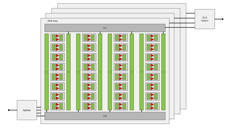
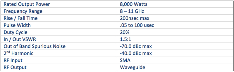
The amplifier is currently configured for water cooling. Air cooled variants are under development. A block diagram of the 8kW amplifier is shown in Figure 2. Typical performance specifications for the 8kW SSPA are as listed in Table 1.
Click image to enlarge
Figure 2: 8kW SSPA Block Diagram
Click image to enlarge
Table 1: 8kW SSPA Typical Performance
The 8kW SSPAs as designed can be combined to produce even higher power levels. ADI is currently developing a module which will combine three of these units to produce a peak power level of 24kW. Other configurations achieving power levels up to 32kW are feasible and are under consideration for further evaluation.
ADI is currently developing an advanced power module, also based on GaN technology, which will double the RF output power of current modules. The module is designed to be hermetically sealed to support operation in extreme environments. This, along with next generation combining structures with reduced insertion loss as compared with current ones, will extend output powers to levels approaching 75 to 100kW. These advanced, high power SSPAs will include control and processor functionality to enable fault monitoring, built in test, remote diagnostic testing, and control of fast, real time bias control circuits for the MMIC devices.
Wideband, continuous wave, high-power amplifiers for electronic warfare
The industry need for very wideband, instantaneous bandwidth coverage at high output power levels is addressed by ADI’s lineup of compact, GaN based solid state amplifiers. Some systems attempt to meet these requirements using “channelized” or multiple amplifiers each covering a portion of the required spectrum feeding a multiplexer. This leads to increased cost, complexity and results in coverage gaps at the frequency crossover points of the multiplexer. In this section we present two amplifiers, one covering the entire VHF through L Band spectrum, and the other covering the microwave spectrum through 18 GHz.
Analog Devices has developed an ultra-small, feature-rich, multi-octave high power amplifier for operation in the VHF band through S-band spectrums. This power amplifier offers high power levels of +46dBm (40W typical) from a nominal input signal of 0dBm with complete coverage between 115MHz through 2000MHz. Packed in a compact housing with physical geometries of 7.3”x3.6”x1.4”, this amplifier includes built-in-test (BIT) functionality for thermal and current overload protection, telemetry reporting and an integrated DC-DC converter for uncompromised RF performance with input supplies ranging from +26V to +30V.
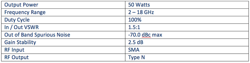
Typical measured data for the VHF thru L band amplifier is shown in Figure 3. To address wideband applications above 2 GHz ADI offers an amplifier producing 50 watts across the entire 2 to 18 GHz band. This amplifier uses commercially available 10 watt GaN MMICs combined using a wideband, low loss combiner circuit. Multiple amplifiers may in turn be combined to develop output powers as high as 200 watts. The driver amplifier chain is also GaN based. The amplifier operates from 48 volts DC and features internal voltage regulator and high speed switching circuits to enable pulsed operation with good pulse fidelity and rise and fall times. Specifications for this amplifier are presented in Table 2.

Click image to enlarge
Figure 3: Output Power vs. Frequency
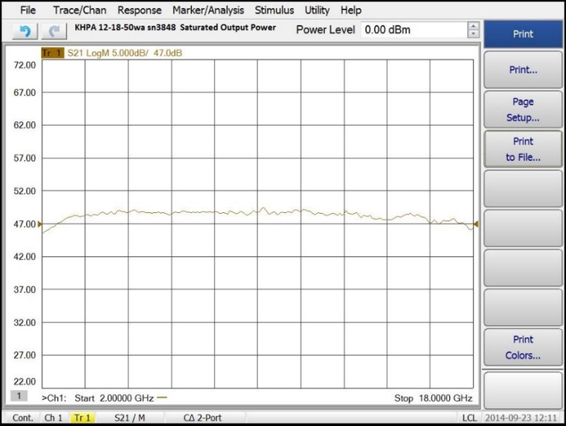
Typical output power vs. frequency performance for this amplifier is shown in Figure 4. This 50-watt amplifier is one of a family of amplifiers covering the 2 – 18 GHz band. ADI also offers a compact, bench top amplifier producing 12 watts, shown in Figure 5, and a rack mount unit developing 100 watts. Other amplifiers offering coverage from 2 – 6 and 6 – 18 GHz are under development.
Clcik image to enlarge
Figure 4: 2 – 18 GHz Amplifier Output Power vs. Frequency

Click image to enlarge
Figure 5: 2 – 18 GHz, 12 Watt Amplifier
ADI is also working to increase the output power of these broadband amplifiers from their current levels to power levels of 200 watts and above, developing modules with increased output power as well as broadband RF power combiners that offer greatly improved combining efficiency and less loss than those used in current products.
The power of GaN
In this article we’ve reviewed several examples of GaN based high power amplifier systems. All of these products offer substantial improvements in output power, efficiency, and reliability over that of product currently deployed. Recurring, per unit costs should continue to drop as more GaN vendors move to larger wafer sizes.
Systems operating at millimeter wave frequencies will see more use of GaN devices as gate lengths are reduced, enabling higher frequency operation. It is clear that the trends that are increasing performance and lowering costs in the field will continue into the future.